%%{init: {'theme': 'base', 'themeVariables': { 'primaryColor': '#2C3E50', 'primaryTextColor': '#fff', 'primaryBorderColor': '#1A252F', 'lineColor': '#2C3E50', 'secondaryColor': '#16A085', 'tertiaryColor': '#E67E22', 'noteTextColor': '#2C3E50', 'noteBkgColor': '#ECF0F1', 'textColor': '#2C3E50', 'fontSize': '16px'}}}%%
graph TD
    subgraph LOWSIDE["Low-Side Switching (N-Channel MOSFET)"]
        VCC1["VCC +12V"]
        LOAD1["Load<br/>(Motor, LED, Relay)"]
        NMOS1["N-MOSFET<br/>Drain"]
        NMOS1S["Source → GND"]
        GPIO1["GPIO 3.3V → Gate<br/>(via 100Ω)"]

        VCC1 --> LOAD1
        LOAD1 --> NMOS1
        NMOS1 --> NMOS1S
        GPIO1 -.Control.-> NMOS1
    end

    subgraph HIGHSIDE["High-Side Switching (P-Channel MOSFET)"]
        VCC2["VCC +12V"]
        PMOS2["P-MOSFET<br/>Source"]
        PMOS2D["Drain"]
        LOAD2["Load<br/>(Sensor, Module)"]
        GND2["GND"]
        GPIO2["GPIO 3.3V → Gate<br/>(inverted logic)"]

        VCC2 --> PMOS2
        PMOS2 --> PMOS2D
        PMOS2D --> LOAD2
        LOAD2 --> GND2
        GPIO2 -.Control.-> PMOS2
    end

    subgraph HBRIDGE["H-Bridge Motor Control (4 MOSFETs)"]
        VCCM["VCC +12V"]
        Q1["Q1 High-side"]
        Q2["Q2 Low-side"]
        MOTOR["DC Motor"]
        Q3["Q3 Low-side"]
        Q4["Q4 High-side"]
        GNDM["GND"]

        VCCM --> Q1
        VCCM --> Q4
        Q1 --> MOTOR
        Q4 --> MOTOR
        MOTOR --> Q2
        MOTOR --> Q3
        Q2 --> GNDM
        Q3 --> GNDM
    end

    subgraph PROTECT["Protection Circuits"]
        FLYBACK["Flyback Diode<br/>(1N4007)<br/>Across inductive load"]
        ZENER["Zener Clamp<br/>(5.1V)<br/>Protects gate"]
        RESISTOR["Gate Resistor<br/>(100Ω)<br/>Limits current"]
    end

    style LOWSIDE fill:#E8F6F3,stroke:#16A085,color:#2C3E50
    style HIGHSIDE fill:#FEF5E7,stroke:#E67E22,color:#2C3E50
    style HBRIDGE fill:#ECF0F1,stroke:#2C3E50,color:#2C3E50
    style PROTECT fill:#FADBD8,stroke:#E74C3C,color:#2C3E50
    style VCC1 fill:#16A085,stroke:#138D75,color:#fff
    style LOAD1 fill:#ECF0F1,stroke:#7F8C8D,color:#2C3E50
    style NMOS1 fill:#2C3E50,stroke:#1A252F,color:#fff
    style VCC2 fill:#E67E22,stroke:#D35400,color:#fff
    style PMOS2 fill:#2C3E50,stroke:#1A252F,color:#fff
    style LOAD2 fill:#ECF0F1,stroke:#7F8C8D,color:#2C3E50
    style VCCM fill:#7F8C8D,stroke:#5D6D7E,color:#fff
    style MOTOR fill:#2C3E50,stroke:#1A252F,color:#fff
    style Q1 fill:#16A085,stroke:#138D75,color:#fff
    style Q2 fill:#16A085,stroke:#138D75,color:#fff
    style Q3 fill:#16A085,stroke:#138D75,color:#fff
    style Q4 fill:#16A085,stroke:#138D75,color:#fff
598 Transistor Selection Guide for IoT
598.1 Transistor Selection Guide for IoT Projects
Choosing the right transistor for your IoT project can be overwhelming with thousands of options. This guide provides a practical framework for selecting transistors based on your specific requirements.
598.1.1 Decision Framework: BJT vs MOSFET
Start here to narrow down your choice between the two main transistor families:
| Question | Choose BJT | Choose MOSFET |
|---|---|---|
| What’s your power budget? | Mains powered, continuous operation OK | Battery powered, need ultra-low power |
| What current are you switching? | < 500mA (BJT adequate) | > 500mA or need low losses |
| What’s your control signal? | Have current available (>1mA) | Limited current (<100µA GPIO) |
| How often does it switch? | Infrequent (<1 kHz) | High frequency (>10 kHz) |
| What’s your experience level? | Beginner (BJT simpler biasing) | Intermediate (MOSFET gate drive trickier) |
Rule of Thumb: For modern IoT projects, MOSFET is usually the better choice due to voltage control (no base current drain), lower power losses (lower Rds(on)), and faster switching.
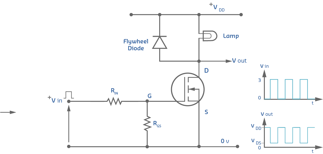
598.1.2 Transistor Switching Circuits for IoT
The most common transistor configurations you’ll encounter in IoT hardware design:
{fig-alt=“Electronics diagram illustrating”Low-Side Switching (N-Channel MOSFET)“,”VCC +12V”, “Load (Motor, LED, Relay)” showing semiconductor components, transistor circuits, diode operation, signal amplification, or switching circuits used in sensor and actuator interfacing for IoT systems.”}
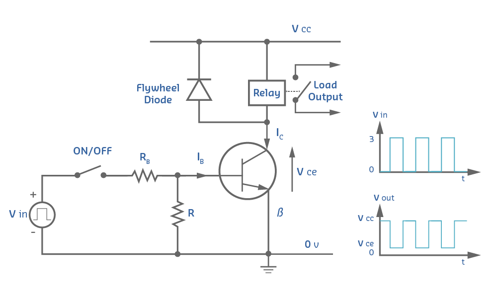
Common transistor switching circuits for IoT: Low-side switching uses N-channel MOSFET with load between VCC and drain, source grounded, GPIO controls gate (most common 80% of applications); High-side switching uses P-channel MOSFET with source at VCC, drain to load, inverted logic (GPIO LOW turns ON) for battery disconnect and sensor power control; H-bridge uses 4 MOSFETs (2 high-side, 2 low-side) enabling bidirectional DC motor control with Q1+Q3 for forward, Q2+Q4 for reverse, requires dead-time to prevent shoot-through; Protection circuits include flyback diodes across inductive loads, Zener clamps for gate overvoltage, and gate resistors to limit current spikes.
Key Insights:
| Circuit Type | When to Use | Advantages | Critical Design Note |
|---|---|---|---|
| Low-Side N-MOSFET | Motors, relays, LEDs, most loads | Simplest, cheapest, direct GPIO control | Load not at ground potential (affects sensors) |
| High-Side P-MOSFET | Battery disconnect, sensor power, reverse polarity protection | Load at ground, true power-off | Inverted logic (LOW=ON), higher Rds(on) |
| H-Bridge | DC motors needing reversing, bidirectional control | Forward/reverse/brake/coast modes | Must implement dead-time (1-5µs), risk of shoot-through |
| Flyback Diode | ALL inductive loads (relays, solenoids, motors) | Protects transistor from voltage spikes (>300V) | Cathode to VCC, anode to GND side of load |
598.1.3 Common IoT Application Transistor Recommendations
Based on real-world IoT projects, here are proven transistor choices for common scenarios:
| Application | Recommended Transistor | Specs | Why This One? | Alternative |
|---|---|---|---|---|
| LED indicator (20mA) | 2N2222 (NPN BJT) | 40V, 600mA, β=100-300 | Cheap ($0.05), easy to bias, overkill specs | BC547 (smaller package) |
| Relay control (50mA coil) | 2N3904 (NPN BJT) or 2N7000 (N-MOSFET) | BJT: 40V, 200mA MOSFET: 60V, 200mA |
Both work well, MOSFET uses less power | BC337 for higher current |
| High-power LED (350mA) | IRLZ44N (N-MOSFET) | 55V, 47A, Rds(on)=19mΩ @ Vgs=5V | Logic-level (works with 3.3V/5V GPIO), low losses | FQP30N06L (cheaper) |
| Motor control (1-3A) | IRF540N or IRLZ44N (N-MOSFET) | 100V, 33A, Rds(on)=44mΩ | Handles high current, low heat generation | IRL540N (logic-level version) |
| Solenoid valve (500mA) | TIP120 (Darlington NPN) or FQP30N06L (N-MOSFET) | Darlington: 60V, 5A, β=1000 MOSFET: 60V, 32A |
Darlington simplest, MOSFET more efficient | TIP122 for higher gain |
| High-side switching (5V) | IRF9540 (P-channel MOSFET) | 100V, 23A, Rds(on)=117mΩ | High-side switching without level shifter | FQP27P06 (lower Rds(on)) |
| Load switching (ultra-low power) | AO3401 (P-channel SOT-23) | 30V, 4A, Rds(on)=35mΩ, leak<1µA | SMD compact, near-zero leakage for battery | Si2333DS (even lower leak) |
| H-bridge motor driver | 4× IRLZ44N (2 high, 2 low) | 55V, 47A, Rds(on)=19mΩ | Logic-level, handles high current, low losses | L298N module (integrated solution) |
| 5V→3.3V level shifter | BSS138 (N-channel SOT-23) | 50V, 200mA, Rds(on)=3.5Ω | Standard for bidirectional I2C/SPI shifting | 2N7000 (through-hole version) |
| Signal amplifier (audio) | 2N3904 (NPN) + 2N3906 (PNP) | Complementary pair for push-pull | Low noise, good for small-signal amplification | BC547/BC557 pair |
SMD vs Through-Hole Trade-Offs: - Through-hole (TO-92, TO-220): Easier for beginners, hand-solderable, good heat dissipation (TO-220 with heatsink) - SMD (SOT-23, SOT-223, DPAK): Compact for production, cheaper in volume, harder to solder by hand
598.1.4 Detailed Selection Criteria
When the simple recommendation table doesn’t fit your needs, use these detailed criteria:
NoteVoltage Rating (V_CE, V_DS)
What to check: Maximum voltage between collector-emitter (BJT) or drain-source (MOSFET)
Selection rule: Choose transistor with voltage rating ≥ 2× your supply voltage for safety margin
Examples: - 5V circuit → ≥10V transistor (2N2222: 40V ✓) - 12V motor → ≥24V transistor (IRF540N: 100V ✓) - 24V industrial → ≥50V transistor (TIP120: 60V ✓)
Common mistake: Using 2N7000 (60V) for 48V system → fails (need 100V+ transistor)
NoteCurrent Rating (I_C, I_D)
What to check: Maximum continuous collector (BJT) or drain current (MOSFET)
Selection rule: Choose transistor with current rating ≥ 2-3× your load current for thermal safety
Examples: - 100mA LED → ≥200mA transistor (2N3904: 200mA ✓) - 1A motor → ≥2A transistor (IRF540N: 33A ✓, huge safety margin) - 10A heater → ≥20A transistor (IRFB3207: 180A ✓)
Thermal derating: At 25°C use full rating, at 85°C derate to 50-70% of rating
Common mistake: “2A motor needs 2A transistor” → overheats (motor stall current may be 5A!)
NotePower Dissipation (P_D)
What to check: Maximum power transistor can dissipate as heat
Calculation: - BJT: P = V_CE(sat) × I_C (saturation) or P = V_CE × I_C (active mode) - MOSFET: P = I_D² × Rds(on) (when ON) or P = V_DS × I_D (switching losses)
Selection rule: Ensure P_dissipation < P_D rating (with heatsink if needed)
Examples:
Switching 2A at 12V with MOSFET:
- Rds(on) = 100mΩ
- P = (2A)² × 0.1Ω = 0.4W
- TO-220 package: 1W without heatsink, 25W with heatsink
- Conclusion: No heatsink needed (0.4W < 1W)

Switching 2A at 12V with BJT:
- V_CE(sat) = 0.5V (typical for saturated BJT)
- P = 0.5V × 2A = 1W
- TO-92 package: 0.5W max
- Conclusion: NEED heatsink or bigger package
Why MOSFETs win: Lower on-resistance → less heat → longer life, smaller package
NoteSwitching Speed (f_T, t_on, t_off)
What to check: How fast can the transistor switch on/off?
Selection rule: For PWM/switching applications, choose transistor with f_T ≥ 10× your PWM frequency
Examples: - 1 kHz PWM (motor speed control) → f_T ≥ 10 kHz (most transistors OK) - 20 kHz PWM (LED dimming, avoid audible whine) → f_T ≥ 200 kHz (2N2222: 300 MHz ✓) - 100 kHz switching (buck converter) → f_T ≥ 1 MHz (specialized switching FETs)
Switching losses: At high frequencies, switching losses dominate. Use MOSFETs with low gate charge (Q_g) for efficiency.
Common mistake: Using slow Darlington (TIP120) for 20 kHz PWM → overheating, poor efficiency
NoteLogic-Level vs Standard Gate Drive (MOSFETs only)
Critical MOSFET selection criterion often overlooked by beginners!
Standard MOSFETs: - Need V_GS = 10-12V to fully turn ON (achieve specified Rds(on)) - IRF540N datasheet: Rds(on) = 44mΩ @ V_GS = 10V - With 5V gate drive: Rds(on) = ~200mΩ (4.5× higher → 4.5× more heat!)
Logic-Level MOSFETs: - Fully turn ON with V_GS = 4.5-5V (works with 3.3V/5V microcontrollers) - IRLZ44N datasheet: Rds(on) = 19mΩ @ V_GS = 5V ✓ - Note the “L” in IRLLZ44N → Logic-level
Selection rule: - 3.3V/5V microcontroller: MUST use logic-level MOSFET (look for “logic-level” or V_GS(th) < 2.5V in datasheet) - 12V+ gate driver: Can use standard MOSFET (often cheaper, lower Rds(on))
Common beginner mistake: “My IRF540N gets really hot even though it’s rated for 33A and I’m only switching 2A” → Using standard MOSFET with 5V gate drive! Solution: Replace with IRLZ44N (logic-level version)
598.1.5 Real-World Example: Choosing Transistor for Smart Garden Irrigation
Requirements: - Control 12V solenoid valve (opening/closing water flow) - Solenoid coil: 12V, 50mA nominal, 200mA inrush current - Controlled by ESP32 GPIO (3.3V, 12mA max) - Battery powered (need low quiescent current) - Outdoor deployment (temperature: -10°C to +60°C)
Decision Process:
Step 1: BJT or MOSFET? - Battery powered → prefer MOSFET (zero gate current) - Load: 200mA → either works, but MOSFET more efficient - Choice: MOSFET
Step 2: Voltage rating? - Solenoid: 12V → need ≥24V rating for safety - Inductive load voltage spikes → 100V rated MOSFET safer - Requirement: V_DS ≥ 30V (prefer 50-100V)
Step 3: Current rating? - Load: 200mA peak → need ≥400mA continuous rating - Requirement: I_D ≥ 500mA (most MOSFETs exceed this)
Step 4: Logic-level or standard? - ESP32 GPIO: 3.3V → MUST be logic-level - Need V_GS(th) < 2V, fully on at V_GS = 3.3V - Requirement: Logic-level MOSFET
Step 5: Package and thermal? - P_dissipation = I² × Rds(on) = (0.2)² × 0.03Ω = 1.2mW - Negligible heat → no heatsink needed - Requirement: Any package (TO-92, SOT-23)
Final Selection: 2N7000 (N-channel MOSFET) - V_DS: 60V ✓ (safe for 12V + inductive spikes) - I_D: 200mA ✓ (exactly matches requirement) - V_GS(th): 2.1V typical ✓ (fully on at 3.3V) - Package: TO-92 ✓ (easy to hand solder) - Cost: $0.10 ✓ (very cheap) - Rds(on): 1.8Ω @ V_GS=4.5V → P = 0.072W ✓ (acceptable losses)
Additional Protection: Add 1N4007 flyback diode across solenoid coil (cathode to +12V, anode to GND) to protect MOSFET from inductive kickback when solenoid turns OFF.
Circuit:
ESP32 GPIO ---[1kΩ]--- Gate (2N7000)
                        Drain --- Solenoid --- +12V
                        Source --- GND

Flyback diode: Cathode (+) to +12V, Anode (-) to Drain
Why NOT alternatives: - BJT (2N2222): Needs base current (~2mA), wastes battery power - IRF540N: Standard gate (not logic-level), won’t fully turn on with 3.3V - Relay: 50mA coil current wasteful for battery, mechanical wear, slower
598.2 Chapter Summary
Semiconductors are the foundation of modern electronics, offering controllable conductivity between conductors and insulators through doping with impurities. N-type semiconductors have excess electrons (negative charge carriers), while P-type semiconductors have excess holes (positive charge carriers). Combining these materials creates diodes and transistors—the building blocks of all digital circuits and microcontrollers.
Diodes are two-layer PN junctions that allow current flow in only one direction, conducting when forward-biased (P-side positive) and blocking when reverse-biased. Applications include rectification (AC to DC conversion), voltage regulation (Zener diodes), light emission (LEDs), and circuit protection (flyback diodes preventing inductive voltage spikes). The forward voltage drop (~0.7V for silicon) must be considered in circuit design.
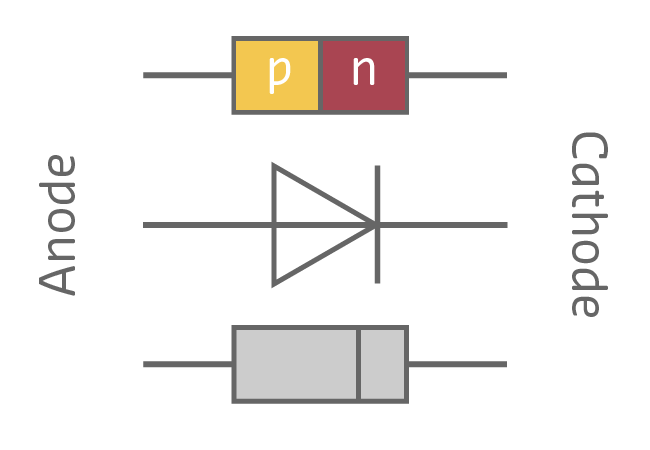
TipAI-Generated Figure: Diode Structure and Symbols (Artistic Rendering)

Diode fundamentals: PN junction structure, schematic symbol, and physical package identification.
Transistors act as electronically controlled switches or amplifiers, enabling digital logic and motor control in IoT devices. BJT (Bipolar Junction Transistors) are current-controlled, where small base current controls large collector current, while FETs (Field Effect Transistors) are voltage-controlled with nearly zero gate current. MOSFETs are the most common type in modern IoT circuits due to low power consumption.
Practical transistor applications in IoT include switching high-current loads (motors, relays, LEDs), level shifting between different voltage domains, and signal amplification. Protection components like flyback diodes, current-limiting resistors, and proper heat sinking ensure reliable operation. Understanding transistor characteristics (saturation voltage, current gain, switching speed) is essential for robust circuit design.
598.3 What’s Next?
Continue to Electronics Summary and Resources for chapter summary, common pitfalls, and visual reference galleries.