%%{init: {'theme': 'base', 'themeVariables': { 'primaryColor': '#2C3E50', 'primaryTextColor': '#fff', 'primaryBorderColor': '#1A252F', 'lineColor': '#2C3E50', 'secondaryColor': '#16A085', 'tertiaryColor': '#E67E22', 'noteTextColor': '#2C3E50', 'noteBkgColor': '#ECF0F1', 'textColor': '#2C3E50', 'fontSize': '16px'}}}%%
flowchart TD
    PURE["Pure Silicon<br/>(4 valence electrons)<br/>Poor conductor"]

    PURE --> NTYPE["N-Type Doping<br/>Add Phosphorus (5e⁻)<br/>Extra electrons"]
    PURE --> PTYPE["P-Type Doping<br/>Add Boron (3e⁻)<br/>Missing electrons (holes)"]

    NTYPE --> NRESULT["N-Type Semiconductor<br/>Majority: Electrons (-)<br/>Minority: Holes (+)"]

    PTYPE --> PRESULT["P-Type Semiconductor<br/>Majority: Holes (+)<br/>Minority: Electrons (-)"]

    style PURE fill:#7F8C8D,stroke:#5D6D7E,color:#fff
    style NTYPE fill:#16A085,stroke:#138D75,color:#fff
    style PTYPE fill:#E67E22,stroke:#D35400,color:#fff
    style NRESULT fill:#ECF0F1,stroke:#16A085,color:#2C3E50
    style PRESULT fill:#ECF0F1,stroke:#E67E22,color:#2C3E50
595 Semiconductors, Doping, and Diodes
595.1 Semiconductors: The Foundation of Electronics
595.1.1 Pure Semiconductors
Common Materials: - Silicon (Si) - 95% of all semiconductors - Germanium (Ge) - Historical use, now rare - Gallium Arsenide (GaAs) - High-frequency applications
Pure semiconductors aren’t very useful because they don’t conduct well at room temperature.
TipAI-Generated Figure: Atomic Structure (Artistic Rendering)

Understanding atomic structure helps explain why silicon (4 valence electrons) makes an ideal semiconductor material.
595.1.2 Doping: Creating Useful Semiconductors
Doping = Adding impurities (dopants) to semiconductors to control conductivity
{fig-alt=“Electronics diagram illustrating”Pure Silicon (4 valence electrons) Poor conductor”, “N-Type Doping Add Phosphorus (5e⁻) Extra electrons”, “P-Type Doping Add Boron (3e⁻) Missing electrons (holes)” showing semiconductor components, transistor circuits, diode operation, signal amplification, or switching circuits used in sensor and actuator interfacing for IoT systems.”}
Doping process showing how pure silicon (4 valence electrons) is transformed into N-type semiconductor by adding phosphorus dopant (5 valence electrons creating excess electrons) or P-type semiconductor by adding boron dopant (3 valence electrons creating holes). N-type has electrons as majority carriers, P-type has holes as majority carriers, enabling controllable conductivity for transistors and diodes.
595.2 N-type and P-type Semiconductors
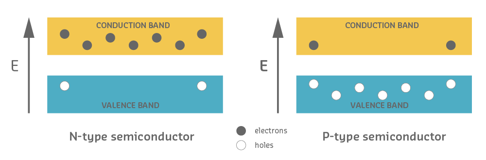
595.2.1 N-type (Negative)
Doping: Add elements with extra electrons (e.g., Phosphorus)
Result: Excess of free electrons (negative charge carriers)
Silicon atom: 4 valence electrons
Phosphorus dopant: 5 valence electrons → 1 extra electron!
Properties: - Majority carriers: Electrons (-) - Minority carriers: Holes (+) - Better conductivity than pure silicon
595.2.2 P-type (Positive)
Doping: Add elements with fewer electrons (e.g., Boron)
Result: Deficit of electrons creates “holes” (positive charge carriers)
Silicon atom: 4 valence electrons
Boron dopant: 3 valence electrons → 1 missing electron (hole)!
Properties: - Majority carriers: Holes (+) - Minority carriers: Electrons (-) - Holes act as positive charge carriers
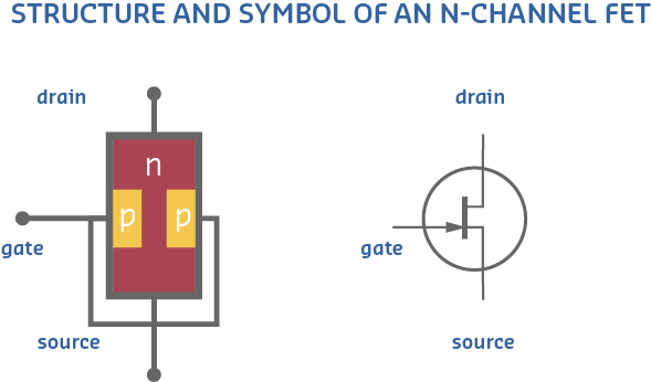
595.2.3 Transistor Types Overview
Understanding the different transistor families helps you select the right component for IoT applications:
%%{init: {'theme': 'base', 'themeVariables': { 'primaryColor': '#2C3E50', 'primaryTextColor': '#fff', 'primaryBorderColor': '#1A252F', 'lineColor': '#2C3E50', 'secondaryColor': '#16A085', 'tertiaryColor': '#E67E22', 'noteTextColor': '#2C3E50', 'noteBkgColor': '#ECF0F1', 'textColor': '#2C3E50', 'fontSize': '16px'}}}%%
graph TD
    ROOT["Transistors<br/>3-Layer Semiconductors"]

    ROOT --> BJT["BJT<br/>Bipolar Junction<br/>Transistor"]
    ROOT --> FET["FET<br/>Field Effect<br/>Transistor"]

    BJT --> NPN["NPN<br/>Current-controlled<br/>β = 50-300"]
    BJT --> PNP["PNP<br/>Current-controlled<br/>β = 50-300"]

    FET --> JFET["JFET<br/>Junction FET<br/>Always-on"]
    FET --> MOSFET["MOSFET<br/>Metal-Oxide FET<br/>Voltage-controlled"]

    MOSFET --> NMOS["N-Channel<br/>Low-side switch<br/>Rds(on) < 100mΩ"]
    MOSFET --> PMOS["P-Channel<br/>High-side switch<br/>Rds(on) > 100mΩ"]

    NPN --> NPNAPP["Applications:<br/>Low-side switching<br/>Signal amplification<br/>Darlington pairs"]

    PNP --> PNPAPP["Applications:<br/>High-side switching<br/>Complementary pairs<br/>Current sources"]

    NMOS --> NMOSAPP["Applications:<br/>Motor drivers<br/>Power switching<br/>90% of IoT usage"]

    PMOS --> PMOSAPP["Applications:<br/>Load switching<br/>Reverse polarity protection<br/>Battery disconnect"]

    style ROOT fill:#2C3E50,stroke:#1A252F,color:#fff
    style BJT fill:#E67E22,stroke:#D35400,color:#fff
    style FET fill:#16A085,stroke:#138D75,color:#fff
    style NPN fill:#ECF0F1,stroke:#E67E22,color:#2C3E50
    style PNP fill:#ECF0F1,stroke:#E67E22,color:#2C3E50
    style JFET fill:#ECF0F1,stroke:#16A085,color:#2C3E50
    style MOSFET fill:#ECF0F1,stroke:#16A085,color:#2C3E50
    style NMOS fill:#ECF0F1,stroke:#16A085,color:#2C3E50
    style PMOS fill:#ECF0F1,stroke:#16A085,color:#2C3E50
    style NPNAPP fill:#FEF5E7,stroke:#E67E22,color:#2C3E50
    style PNPAPP fill:#FEF5E7,stroke:#E67E22,color:#2C3E50
    style NMOSAPP fill:#E8F6F3,stroke:#16A085,color:#2C3E50
    style PMOSAPP fill:#E8F6F3,stroke:#16A085,color:#2C3E50
{fig-alt=“Electronics diagram illustrating”Transistors 3-Layer Semiconductors”, “BJT Bipolar Junction Transistor”, “FET Field Effect Transistor” showing semiconductor components, transistor circuits, diode operation, signal amplification, or switching circuits used in sensor and actuator interfacing for IoT systems.”}
Transistor types taxonomy showing two main families: BJT (Bipolar Junction Transistors) are current-controlled devices with NPN and PNP types offering current gain β=50-300, used for signal amplification and switching; FET (Field Effect Transistors) are voltage-controlled with JFET (always-on devices) and MOSFET (metal-oxide semiconductor) types, where N-channel MOSFETs dominate IoT applications (90% usage) for motor drivers and power switching with low on-resistance Rds(on)<100mΩ, while P-channel MOSFETs handle high-side switching and battery disconnect circuits.
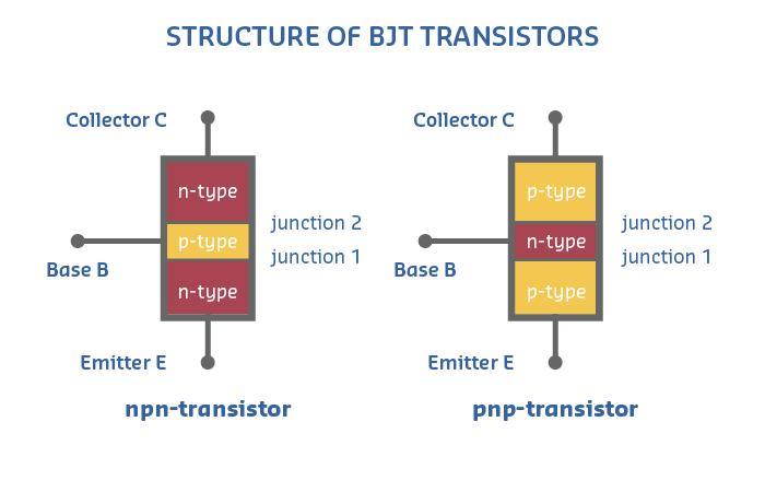
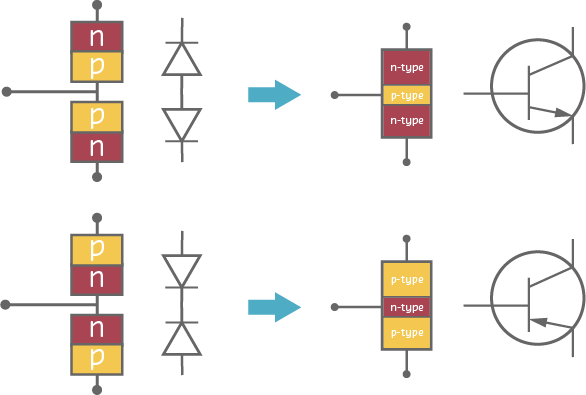
BJT transistor diode model showing NPN and PNP as two back-to-back PN junctions with schematic symbols


NoteCross-Hub Connections
Explore More Electronics Resources:
- Simulations Hub - Try interactive circuit simulators (TinkerCAD, Falstad) to build transistor switches and test diode circuits without physical components
- Videos Hub - Watch visual explanations of semiconductor physics, PN junction behavior, and transistor operation at the atomic level
- Quizzes Hub - Test your understanding of BJT vs MOSFET selection, power dissipation calculations, and circuit design decisions
- Knowledge Gaps Hub - Clarify common confusions about gate drive voltage, current vs voltage control, and thermal management
Why This Matters: Electronics fundamentals connect to nearly every IoT topic. Understanding transistors enables you to design sensor interfaces (signal conditioning), control actuators (motor drivers), optimize power consumption (load switching), and troubleshoot hardware issues (thermal problems, shoot-through).
WarningCommon Misconception: “All MOSFETs Work with 3.3V/5V GPIO”
The Misconception: Many beginners assume any MOSFET can be driven directly from microcontroller GPIO pins (3.3V or 5V), leading to circuits that “sort of work” but run hot, waste power, and fail prematurely.
The Reality with Real Numbers: Standard MOSFETs require Vgs = 10-12V to fully turn ON and achieve their datasheet specifications. When driven with insufficient gate voltage, they operate in the linear region with dramatically higher on-resistance.
Real-World Impact (IRF540N Example): - Datasheet spec: Rds(on) = 44mΩ @ Vgs=10V - With 5V gate drive: Rds(on) = 200mΩ (4.5× higher!) - Switching 2A load: - Expected power: (2A)² × 0.044Ω = 0.18W (cool) - Actual power: (2A)² × 0.2Ω = 0.8W (hot!) - TO-220 package without heatsink: 1W max → MOSFET runs at 80°C → premature failure
Measured in Real Projects: A student designed a smart fan controller using IRF540N driven from 5V Arduino. Initial testing worked fine for 10 minutes, but after 30 minutes the MOSFET reached 95°C and the fan speed dropped 40% due to voltage drop across the partially-on MOSFET. After switching to IRLZ44N (logic-level), temperature dropped to 35°C and fan ran at full speed.
The Solution: Always check the Vgs specification in datasheets: - Logic-level MOSFETs: Vgs(th) < 2.5V, fully on at 4.5-5V (look for “L” in part number: IRLZ44N) - Standard MOSFETs: Vgs(th) = 2-4V, but require 10V for rated Rds(on)
Cost of This Mistake: - Wasted heat: 0.8W - 0.18W = 0.62W continuous loss - Battery life: For a 2A load running 50% duty cycle, that’s 7.4Wh/day wasted → 1000mAh battery dies 3× faster - Component damage: Thermal stress reduces MOSFET lifetime from 100,000 hours to <10,000 hours - Debugging time: Students typically spend 2-4 hours troubleshooting “hot MOSFET” before discovering gate voltage issue
Key Takeaway: When selecting MOSFETs for microcontroller projects, ALWAYS verify Rds(on) at YOUR gate voltage (not the datasheet headline spec). Add 50% safety margin for thermal calculations. Logic-level MOSFETs cost the same ($0.50) but save hours of debugging and prevent field failures.
595.3 Knowledge Check
Test your understanding with these questions.
595.4 What’s Next?
Continue to Transistor Selection Guide to learn how to choose the right transistor for your IoT projects.