20 Sampling and Aliasing
Sample Rate, Aliasing, Resolution, and Review Evidence
20.1 In 60 Seconds
An ADC makes a timed digital record of a changing analog voltage. A trustworthy sample plan starts with the physical signal, limits misleading high-frequency content before conversion, samples fast enough with margin, and records the range, reference, bit depth, timestamp policy, and validation evidence that make each code meaningful.
20.2 Start With the Story
Start with a physical signal that is noisy, delayed, sampled, quantized, calibrated, filtered, packed, and finally sent as a number someone will trust. The core idea in Sampling and Aliasing is simple: signal processing is the bridge between the physical world and digital evidence, so every sampling, ADC, filter, and calibration choice changes the value that leaves the device. This page focuses that idea on Layered ADC fundamentals chapter covering sampling, aliasing, anti-alias filtering, resolution fit, and review evidence for IoT sensor pipelines. In everyday IoT, temperature drift, vibration spikes, audio snippets, and lab traces all become decisions only after their limits and uncertainty are made visible. Start simple: trace one measurement through the chain, keep the raw-to-processed evidence, and move advanced math into the deeper review only when the simple chain no longer explains the result.
20.3 What the ADC Promises
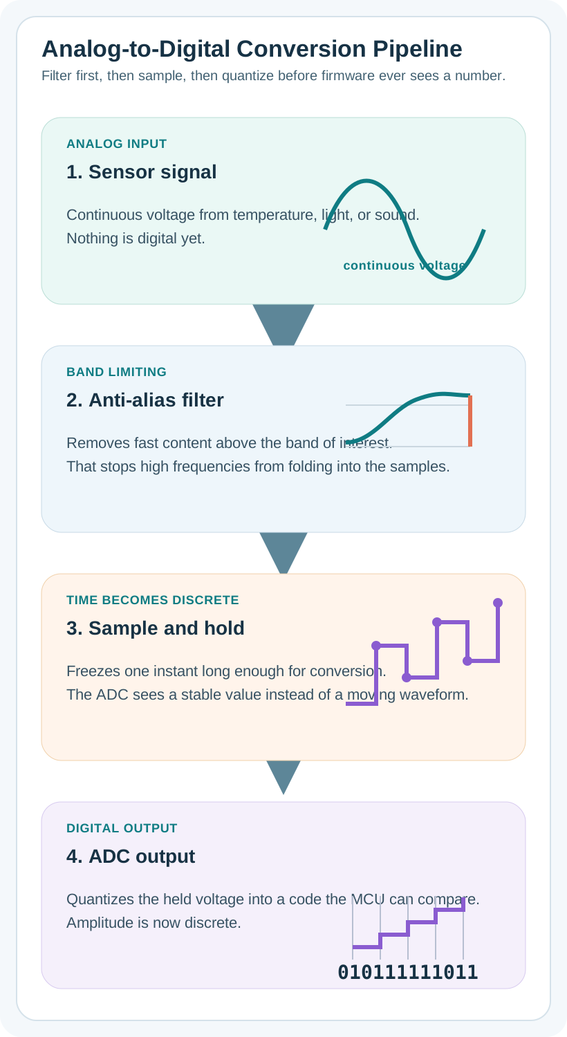
An analog-to-digital converter, or ADC, is the snapshot gate between the physical world and the firmware record. A sensor produces a changing voltage. The ADC samples that voltage at scheduled moments and stores each result as a number.
The important idea is not “sample as fast as possible.” The important idea is trust: a digital sample should still mean the physical thing it claims to mean.
If you only need the intuition, this layer is enough: choose a snapshot speed that is fast enough for the real signal, block misleading high-frequency content before it reaches the ADC, and use enough resolution to see the meaningful voltage changes.
Think of a flipbook. If you photograph a moving wheel often enough, the pages show the wheel turning in the correct direction. If you take too few photos, the same wheel can look slower, stopped, or even reversed. That false motion is aliasing. In ADC work, aliasing can turn high-frequency vibration, electrical noise, or switching ripple into a believable low-frequency pattern.
For example, an irrigation pump monitor might use a 0.5 V to 4.5 V pressure transducer on an STM32 or ESP32 SAR ADC. The dashboard may only need one pressure value each second, but the ADC path still needs to preserve pump ripple, cavitation pulses, and mains-coupled noise before the firmware decides what to summarize. A defensible design may sample around hundreds of samples per second, put an RC or active low-pass filter before the ADC input, and then report a one-second pressure statistic with a timestamp and scale factor. If the firmware sampled once per second directly, the data table would still fill with numbers, but a fast pressure pulse or electrical ripple could fold into a false slow drift.
The One-Minute ADC Decision
Name the useful signal
Start with the physical change the system must preserve, such as room temperature drift, motor vibration, or a pressure pulse.
Protect the sample
Put analog conditioning and anti-alias filtering before conversion so unwanted fast content does not become false evidence.
Record the meaning
Keep the sample rate, voltage range, reference, bit depth, timestamp policy, and validation notes together.
Beginner Examples
- A greenhouse temperature sensor may only need one trustworthy reading every few seconds because the room changes slowly.
- A vibration monitor may need hundreds or thousands of readings per second because the useful fault pattern changes quickly.
- A higher-resolution ADC does not fix a wrong sample rate. More digits can still describe the wrong waveform.
Aliasing Warning Knowledge Check
If this gives you enough to recognize the risk, you can stop here. Continue to Practitioner when you need to design or review the sample path.
20.4 Apply It: Build the ADC Sample Plan
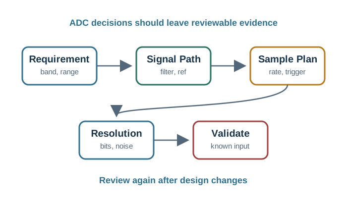
The practical ADC workflow starts with the signal requirement and ends with a short review record. The record matters because a sample rate that made sense in the lab can become wrong after a sensor, filter, enclosure, timer, or power rail changes.
Walkthrough: From Sensor Voltage to Digital Evidence
- State the measurement. Name the physical quantity, expected range, fastest useful change, and acceptable delay.
- Condition the voltage. Scale or shift the sensor output so it fits the ADC input range without clipping or wasting most codes.
- Filter before sampling. Place the anti-alias boundary in the analog path. Digital filters cannot reliably remove content after it has folded into the sampled band.
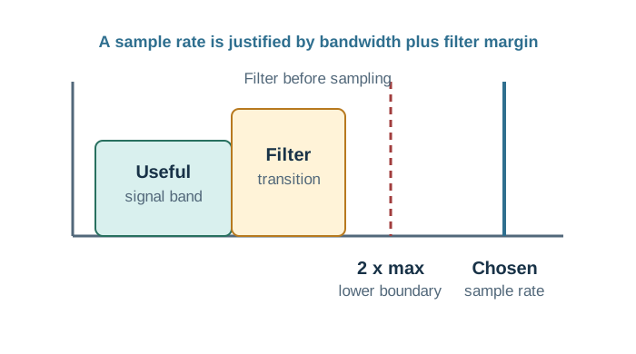
- Choose the sample rate. Start above twice the highest useful frequency, then add margin for filter rolloff, clock tolerance, jitter, and validation uncertainty.
- Check resolution. Make sure one ADC code step is smaller than the meaningful physical change and larger than pure noise.
- Validate and record. Use a known input, reference capture, or repeatable field test to prove the code record still maps to the physical signal.
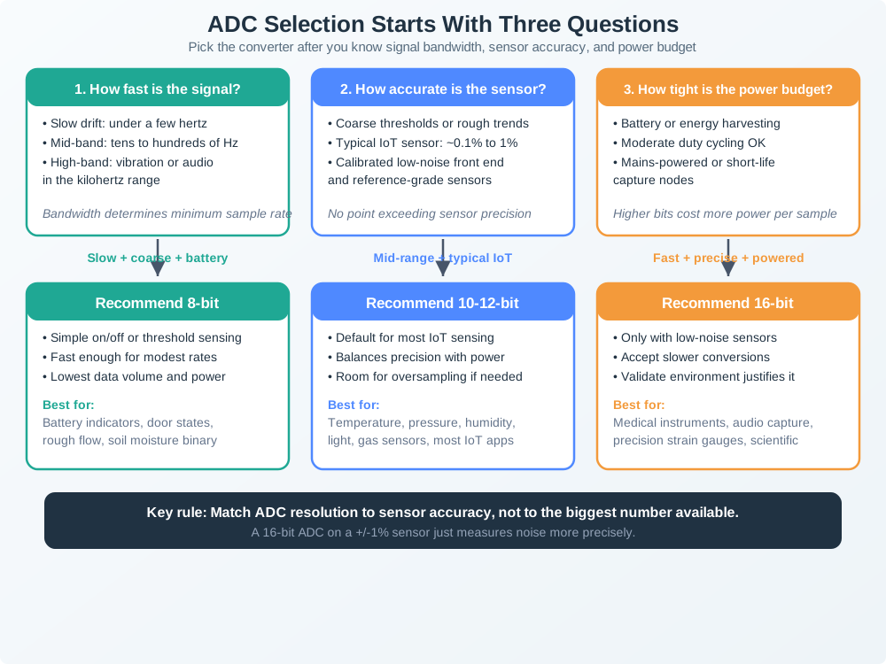
An ADC selection guide keeps three reviews separate. Signal bandwidth drives the sample-rate and anti-alias plan; sensor accuracy and noise decide whether extra bits are useful; power budget constrains whether a faster or higher-resolution converter is practical for a battery device. Treat those as linked engineering choices instead of selecting the largest bit depth on the data sheet.
Worked Example: Temperature Sensor on a 12-Bit ADC
Assume a temperature sensor produces 10 mV for each 1 degree C, and the conditioned output spans 0.1 V to 1.75 V. A 12-bit ADC using a 3.3 V reference has 4096 possible codes.
The calculation says the ADC has enough amplitude detail for many temperature tasks. It does not prove that the sample rate, reference stability, or calibration are good. Those are separate gates.
Try It: Sampling and Aliasing Visualizer
Use the ADC visualizer to move the signal frequency and sample rate. Watch the sample points thin out as the sample rate approaches the signal, then cross the Nyquist boundary to see the false lower-frequency pattern.
Incremental Practice
Beginner
For a slowly changing environment reading, justify why a low sample rate still preserves the useful signal.
Intermediate
For a vibration signal up to 40 Hz, record why the mathematical lower boundary is above 80 samples/s and why the real design needs more margin.
Advanced
Inject a known high-frequency component before the ADC and verify that the analog filter keeps it from folding into the band of interest.
Sample-Rate Review Knowledge Check
If your job is to choose a defensible sample rate and record why it works, you can stop here. Continue to Under the Hood for the formulas behind the review.
20.5 Under the Hood: Math, Limits, and Failure Modes
The deeper layer explains why the practitioner workflow separates sampling, filtering, resolution, and evidence. Each gate answers a different physical question.
Sampling Boundary
The Nyquist rule gives the minimum sampling boundary for a highest useful frequency:
f_s > 2 f_max
This boundary assumes the signal above the useful band has been removed before sampling. Real anti-alias filters have transition bands. A practical design usually samples faster than the bare minimum so the filter has room to attenuate unwanted content.
Alias Frequency
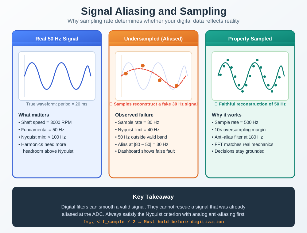
When a sinusoidal component at frequency f is sampled at f_s, a useful way to estimate the folded frequency is:
f_alias = |f - f_s x round(f / f_s)|
-
A
90 Hzsignal sampled at100 samples/saliases to10 Hz. -
A
1200 Hzcomponent sampled at1000 samples/saliases to200 Hz. - Two different high-frequency components can fold into the same apparent low-frequency band, which makes post-processing ambiguous.
Resolution and Quantization
For an ideal ADC with reference voltage V_ref and N bits:
LSB = V_ref / 2^N
The ideal quantization error is within plus or minus half an LSB. For a 12-bit, 3.3 V ADC, one LSB is about 0.806 mV, so the ideal quantization uncertainty is about +/-0.403 mV.
Ideal signal-to-quantization-noise ratio is often approximated as:
SNR_ideal = 6.02N + 1.76 dB
For 12 bits, that is about 74 dB. Real systems often deliver fewer effective bits because of input noise, reference drift, source impedance, aperture jitter, layout coupling, and calibration error. Effective number of bits can be estimated from a measured SNR:
ENOB = (SNR_measured - 1.76) / 6.02
Phoebe’s Why
An ADC does two separate physical operations. First it samples in time, so the analog waveform is multiplied by a clock and copied in frequency around every multiple of \(f_s\). If adjacent copies overlap, a real fast component masquerades as a slow one. Second it quantizes in voltage, so the sample is rounded onto one of \(2^N\) bins. The anti-alias filter protects the time story before sampling; the reference voltage and bit depth set the smallest voltage story the code can tell.
The Derivation
Sampling every \(T_s\) seconds gives \(f_s=1/T_s\). In frequency, the sampled spectrum repeats:
\[X_s(f)=f_s\sum_k X(f-kf_s)\]
For a signal limited to \(|f|\le f_{max}\), neighbouring copies just avoid overlap when
\[f_s-f_{max}\ge f_{max}\]
so
\[f_s\ge 2f_{max}\]
Anything above the safe band folds to the nearest sampled copy:
\[f_{alias}=|f_{signal}-k f_s|\]
For an \(N\)-bit ADC, the bin width is
\[q=\frac{V_{ref}}{2^N}\]
Uniform rounding error has
\[\sigma_q^2=\frac{q^2}{12}\]
and a full-scale sine gives the ideal limit
\[\mathrm{SNR}_{dB}=6.02N+1.76\]
Worked Numbers: This Chapter’s ADC Plan
- 40 Hz signal boundary: the review note’s useful component needs \(f_s\ge 2(40)=80.0\) samples/s before practical filter margin is added.
- 90 Hz into 100 samples/s: \(k=\mathrm{round}(90/100)=1\), so \(f_{alias}=|90-100|=10.0\) Hz.
- 1200 Hz into 1000 samples/s: \(k=1\), so \(f_{alias}=|1200-1000|=200\) Hz, matching the chapter’s warning.
- 12-bit, 3.3 V ADC: \(q=3.3/4096=0.0008057\) V \(=0.806\) mV; half an LSB is \(0.403\) mV.
- Temperature scale: with 10 mV per degree C, one code is \(0.806/10=0.0806\) degree C.
- Conditioned span: \(1.75-0.1=1.65\) V, so the span covers \(1.65/3.3=0.500\) of the ADC range, or \(1.65/0.0008057\approx 2048\) codes.
- Ideal 12-bit SNR: \(6.02(12)+1.76=74.0\) dB before reference drift, noise, jitter, and calibration error reduce the real evidence.
Review Record
Common Pitfalls
- Treating Nyquist as the final answer. The rule gives a lower boundary. It does not choose the filter, margin, validation method, or timing policy.
- Trying to remove aliasing after conversion. Once high-frequency content folds into the sampled band, software may not know which low-frequency pattern is real.
- Buying more bits before checking noise. Extra resolution can create precise-looking numbers that only describe reference drift, noise, or poor range use.
- Ignoring timestamp policy. A correct voltage code is not enough if the system cannot prove when the sample was taken.
Alias Frequency Knowledge Check
Aliasing Symptom Diagnosis
Analog and Digital Filter Boundary
At this depth, the ADC decision is a chain of limits: analog bandwidth, filter attenuation, sampling rate, reference, noise, timing, and validation. A trustworthy sample plan records each limit instead of treating the ADC code as self-explanatory.
20.6 Summary
- ADC design starts with the signal requirement, not the fastest available sample rate.
- Nyquist gives a lower boundary, while real designs need filter and implementation margin.
- Aliasing creates false patterns that can survive into dashboards and analytics.
- Anti-alias filtering must happen before sampling because digital cleanup cannot reliably undo folded content.
- Resolution depends on the whole signal path: range, noise, reference, timing, and calibration.
- A review record keeps the design reproducible when sensors, firmware, filters, or deployment conditions change.
A trustworthy ADC path is evidence-led: useful bandwidth, analog filtering, sample timing, range, reference, resolution, and validation all have to agree.
20.7 See Also
Quantization and Digital Filtering
Review amplitude resolution, code steps, and digital filtering after conversion.
Sensor Dynamics and Response
Connect ADC sampling decisions to the sensor's physical response time and bandwidth.