20 Power Management and Interfaces
20.1 Start With the Battery and Port
Power and interface choices become concrete when you picture a field technician holding the device. How is it powered, how long should it last, which port exposes data or debug access, and what happens when a cable, battery, sensor, or radio module changes?
Start with that physical story. The architecture needs evidence that power states, connectors, buses, protection, service access, and interface ownership support the deployment instead of becoming hidden failure points.

Phoebe’s Why
This chapter is right to insist that ADC range, reference, filter, and sample timing all get proven together, because they answer two different physical questions that both have to hold before a reading can be trusted. The first is a counting question: an N-bit converter can only report \(2^N\) distinct codes across the reference span, so every reading carries a fixed rounding error no measurement can remove. The second is a timing question: the voltage on the ADC’s tiny sampling capacitor has to physically finish charging through the sensor’s source resistance before the converter looks at it, or the reading is stale, not just rounded. The valve node’s own low-pass filter is doing a third job on top of both – keeping any signal faster than the sample rate from folding back into the measurement as fake low-frequency energy.
The Derivation
Quantization step and its noise power for an \(N\)-bit converter over reference span \(V_{ref}\):
\[q = \frac{V_{ref}}{2^N}, \qquad P_{noise} = \frac{q^2}{12}, \qquad \mathrm{SNR(dB)} = 6.02N + 1.76\]
Nyquist minimum sample rate for a signal of bandwidth \(f_{max}\), and why an anti-alias filter must precede the ADC:
\[f_s \geq 2f_{max}\]
RC settling of the source-impedance-and-sample-capacitor network to within \(\pm\tfrac12\) LSB:
\[\tau = R_{source}C_{s/h}, \qquad t_{settle} \approx (N+1)\ln 2\times\tau\]
Worked Numbers: The Valve Node’s Own Position-Feedback ADC
The chapter names the position-feedback ADC and its range clamp and low-pass filter but not a bit width, reference, or source impedance, so take catalog-typical figures for the STM32L/nRF52-class controller the chapter itself names: 12-bit SAR ADC, \(V_{ref}=3.3\) V, \(5.0\) pF sample-and-hold capacitance.
- Quantization: \(q = 3.3/4096 = 0.806\) mV; noise power \(= q^2/12 = 5.41\times10^{-8}\ \mathrm{V}^2\); \(\mathrm{SNR} = 6.02(12)+1.76 = 74.0\) dB – the fixed rounding floor no filtering removes.
- Nyquist, for a catalog-typical slow motorized valve actuator (few-Hz position bandwidth, \(f_{max}=5.0\) Hz): minimum sample rate \(=2\times5.0=10.0\) Hz; a practical 10x-oversampled schedule would run at \(50.0\) Hz, giving the filter real rolloff margin instead of sampling right at the Nyquist edge.
- Settling, light divider (catalog-typical \(10\,\mathrm{k}\Omega\) position-pot-plus-protection source): \(\tau = 10{,}000\times5.0\text{pF} = 50.0\) ns; settling to \(\pm\tfrac12\) LSB needs \((13)\ln2 \approx 9.01\,\tau = 451\) ns – trivially fast against any realistic acquisition window.
- Settling, heavier divider (catalog-typical \(100\,\mathrm{k}\Omega\) surge-protection resistor, exactly the kind of ESD network this chapter flags): \(\tau = 500\) ns, settling time \(= 4.51\ \mu\)s – a full order of magnitude slower, and now large enough to compete with a typical MCU’s default ADC acquisition window if the firmware does not budget for it.
The 10x jump in settling time between those two otherwise-reasonable protection choices is exactly why the chapter treats “source impedance” and “filter settling” as their own line items: a resistor value chosen purely for ESD margin can silently outrun the sample-and-hold window and hand the converter a reading that has not finished charging, no matter how many quantization bits the datasheet advertises.
20.2 Overview
IoT hardware touches the physical world through supply rails, sensors, actuators, and communication buses. Small mistakes at those boundaries create field failures: a floating input wakes a device repeatedly, a wake pin cannot run from the retained rail, an actuator glitches during boot, or a sensor output exceeds the controller input range.
This chapter gives a decision method for power management and device interfaces. It is intentionally platform-neutral: use the same checks whether the design is a small controller board, an industrial node, a wearable device, or a gateway-supervised sensor.
20.3 Learning Objectives
By the end of this chapter, you should be able to:
- build a power-state ledger for boot, active work, idle wait, sleep, fault, service, and update modes;
- connect wake sources, retained data, and safe output states to the device mission;
- select GPIO, ADC, PWM, I2C, SPI, or UART based on signal measurements rather than habit;
- identify voltage-domain, pull-up, debounce, level-shift, and protection needs at each boundary;
- write an interface decision record that can be tested, serviced, and reviewed when requirements change.
20.4 Power and Interface Decision Route
Evaluate power and interfaces together. A bus that works on a bench can still fail a field device if it forces the wrong rail to stay powered, wakes too often, or leaves an actuator in an unsafe state during reset.
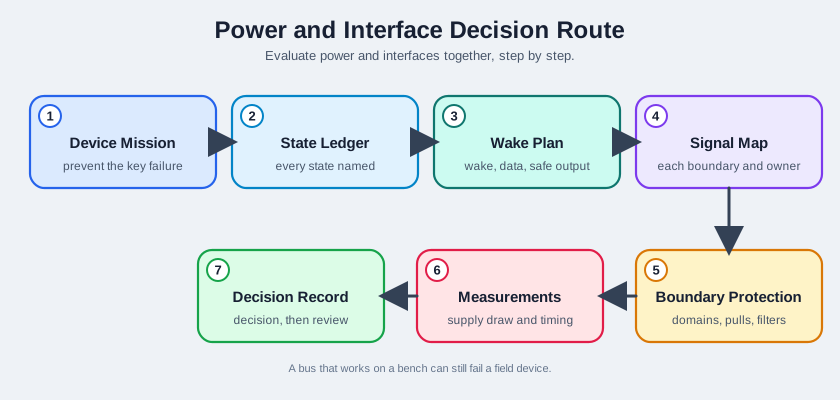
Use this route:
- Define the physical role and the failure the device must prevent.
- List all states the device can enter, including service and update modes.
- Assign wake sources, retained data, and safe outputs to each state.
- Map every signal boundary and decide which component owns it.
- Check voltage domains, pulls, filtering, debounce, isolation, and surge protection.
- Measure the supply draw and timing that the design depends on.
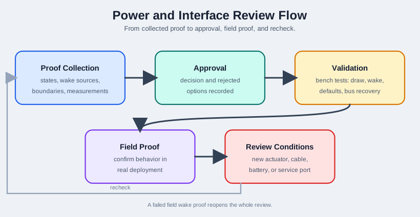
- Record the decision, rejected options, validation tests, and review conditions.
20.5 State Ledger
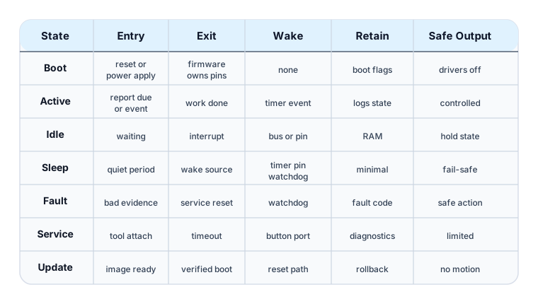
A power design is traceable only when every state has a name, entry condition, exit condition, draw estimate, retained data, and output rule.
20.5.1 Boot
The device starts clocks, memory, peripherals, and output defaults. Outputs should remain safe until firmware explicitly owns them.
20.5.2 Active Work
The device samples, computes, drives actuators, writes state, or transmits. This state should be short and bounded.
20.5.3 Idle Wait
The device is ready but not doing useful work. Timers, interrupts, and bus events should decide whether this state is acceptable.
20.5.4 Sleep or Retention
Most logic is off or paused. Only wake logic and required retained state remain available.
20.5.5 Fault
The device enters a safe behavior after brownout, sensor failure, watchdog reset, stuck bus, or invalid output feedback.
20.5.6 Service and Update
The device exposes diagnostics, update, calibration, or recovery paths. These modes need their own power and interface rules.
20.6 Wake and Retention Plan
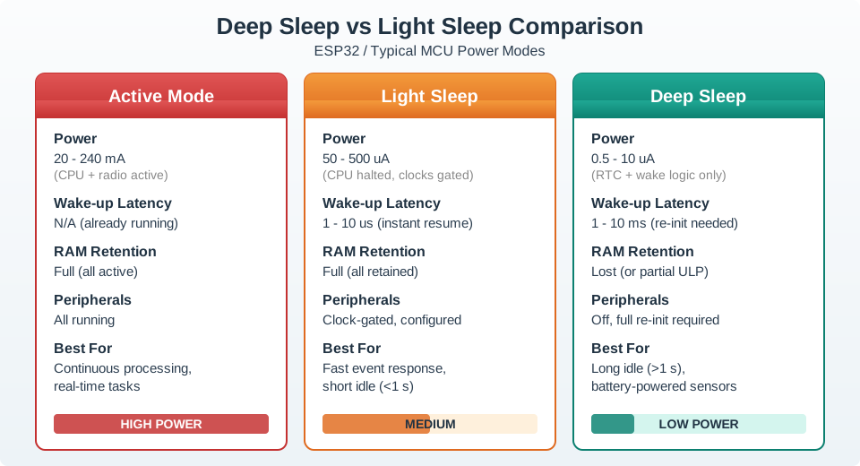
Sleep is useful only when the device can wake for the right reason and recover enough state to act correctly. Treat wake behavior as a signal route, not as a firmware checkbox.
Key questions:
- Which events may wake the device: timer, threshold, button, bus event, radio event, watchdog, or external alarm?
- Is the wake source powered from a rail that remains available in the chosen state?
- Does the wake signal need pull-up, pull-down, debounce, filtering, or edge selection?
- Which data must survive sleep: calibration, sequence number, security material, last safe output, error counter, or time base?
- What is the first safe action after wake before the full application is running?
20.7 Interface Ownership
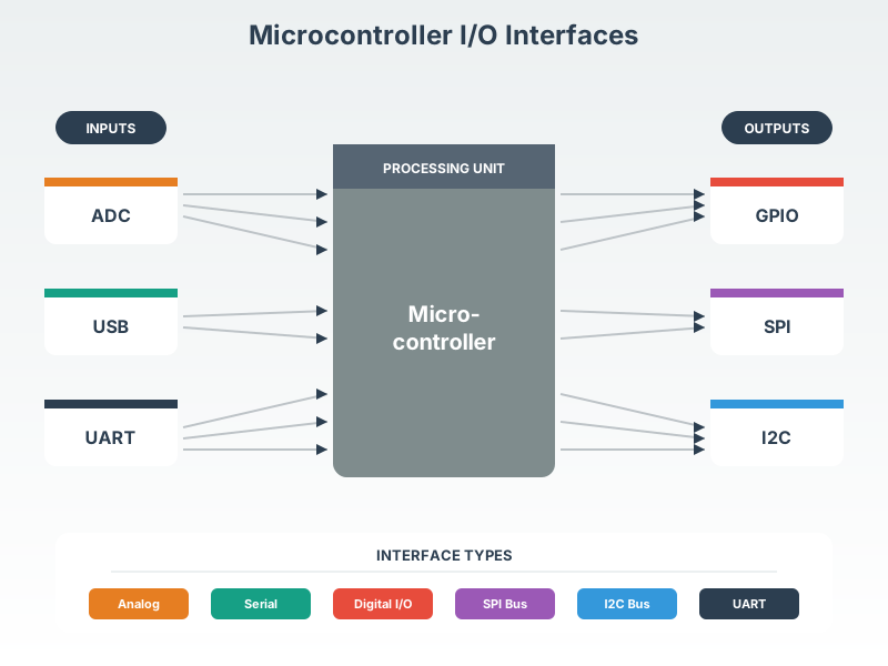
Every signal should have a clear owner. Ambiguous ownership causes double-driving, unsafe defaults, timing faults, and service confusion.
| Interface | Typical Use | Boundary Proof |
|---|---|---|
| GPIO input | Buttons, limit switches, alarms, data-ready pins | Idle level, pull method, debounce, wake capability, input range |
| GPIO output | Enables, LEDs, relays through drivers, chip selects | Boot default, drive strength, fault state, output feedback |
| ADC | Analog sensors, battery monitor, signal feedback | Input range, source impedance, reference rail, filter, sample timing |
| PWM | LED dimming, motors through drivers, valve or fan control | Frequency, duty range, output driver, fail-safe level, audible or thermal limits |
| I2C | Short-board sensor buses and simple peripherals | Pull-up rail, bus length, address plan, stuck-bus recovery |
| SPI | Higher-rate sensors, displays, converters, storage | Chip-select ownership, mode, clock margin, bus sharing, trace length |
| UART | Debug, modems, serial modules, boot console | Baud plan, flow control, wake behavior, service access, isolation needs |
20.8 Signal Boundaries
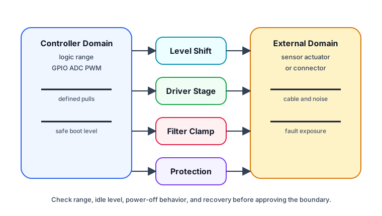
Signal compatibility is a boundary decision. A signal is not approved just because the connector fits.
Check these boundary details:
- Voltage domain: Confirm the signal never exceeds the receiver’s allowed range in normal, boot, sleep, service, and fault states.
- Pull behavior: Define whether the line is pulled high, pulled low, actively driven, tri-stated, or held by an external circuit.
- Level shifting: Use a level shifter, divider, isolator, or open-drain arrangement when two domains use different logic ranges.
- Drive path: GPIO pins should not directly drive high-load actuators. Use a driver stage with flyback or transient protection when needed.
- Analog quality: ADC inputs need source impedance, reference rail, filter, and sample timing proof.
- Protection: External connectors need electrostatic, surge, reverse-polarity, and miswire protection appropriate to the environment.
- Power-off behavior: A powered external module must not back-feed an unpowered controller through signal pins.
20.9 Supply Draw Ledger
Supply draw is a measured state ledger. Estimates are useful early, but approval should depend on measured draw for the modes the device will actually use.
Use a simple weighted model: average draw is the sum of each state draw multiplied by that state’s fraction of the reporting cycle.
The ledger should include:
- state name and trigger;
- expected duration or fraction of the reporting cycle;
- measured supply draw for the whole device, not only the controller;
- rail dependencies, including sensors, radio, storage, converters, pull-ups, and indicators;
- wake delay and time spent returning to useful work;
- environmental margin for temperature, battery age, and sensor tolerance;
- validation method and measurement instrument.
The active portion often dominates even when it is brief. A radio join, actuator burst, sensor warm-up, flash write, or display refresh can outweigh long sleep intervals. Measure those bursts at the device input so the ledger includes converter loss and peripheral behavior.
20.10 Choosing a Bus
Interface selection should follow the signal need.
20.10.1 Use GPIO When
The signal is binary, event-driven, or used for a simple enable. Confirm idle level, wake capability, and safe state before approval.
20.10.2 Use ADC When
The physical value is analog and the required resolution survives sensor tolerance, noise, input range, and reference behavior.
20.10.3 Use PWM When
The output can be controlled by a duty pattern through a proper driver. Confirm frequency, output stage, and safe shutdown behavior.
20.10.4 Use I2C When
Multiple low-rate board-level devices share a short bus. Confirm pull-up rail, addresses, bus recovery, and sleep-state behavior.
20.10.5 Use SPI When
The device needs faster synchronous transfers or deterministic chip-select ownership. Confirm mode, line length, and shared-bus rules.
20.10.6 Use UART When
The module or service port expects a serial stream. Confirm wake, flow control, boot messages, and debug exposure.
20.11 Serial Interface Boundary Addendum
Choose I2C, SPI, or UART from signal measurements, wiring conditions, timing, and recovery behavior. The bus choice should stay connected to the same power and interface decision record used for GPIO, ADC, PWM, and service access.
| Interface | Fit proof | Failure mode to test |
|---|---|---|
| I2C | Short shared board-level bus, low-rate sensors, address map, pull-up rail, capacitance margin, and clock-stretching behavior. | Duplicate fixed addresses, missing pull-ups, cold-start readings, noise on an enclosure path, and stuck-bus recovery after brownout or reset. |
| SPI | Predictable burst transfers for flash, displays, data converters, or high-rate sensors with explicit chip-select ownership. | Wrong clock mode, inactive device driving the shared line, reset during transfer, partial transaction, trace-length margin, and not-ready behavior. |
| UART | Point-to-point module, debug, service, modem, or boot-console stream with clear baud, framing, ground reference, and message boundary rules. | TX/RX crossover errors, incompatible logic level, boot-log exposure, burst flow-control loss, long noisy service leads, and missing recovery commands. |
| Field boundary | Any bus or service port that leaves the board, crosses noisy wiring, or reaches field-accessible connectors. | Need for isolation, protection, transceiver choice, authentication or physical-access assumption, timeout, and safe output behavior during service. |
A mixed design is normal: I2C for short local sensors, SPI for burst peripherals, and UART for service or module links. The design is acceptable only when each link has its own pin, voltage, timing, logging, and recovery proof.
20.12 Walkthrough: Remote Water Valve Node
Consider a remote water valve node that closes a valve when a leak sensor trips and reports periodic health data to a gateway. The device must sleep for long intervals, wake immediately on leak detection, keep the valve safe during reset, and allow service staff to test the actuator at the site.
State ledger
| State | Entry Condition | Exit Condition | Required Proof |
|---|---|---|---|
| Boot | Battery inserted or watchdog reset | Firmware owns outputs | Valve driver disabled by hardware default |
| Sleep | No leak, no service session, no report due | Timer, leak interrupt, service button | Leak wake pin powered and debounced |
| Active sample | Scheduled health report | Reading accepted or marked suspect | Sensor rail enabled only during sample window |
| Leak response | Leak interrupt asserted | Valve closed and report queued | Wake latency and driver enable verified |
| Fault | Brownout, stuck bus, actuator feedback mismatch | Local reset or service action | Valve moves to safe state |
| Service | Service button and authenticated tool | Timeout or service close | UART isolated from external wiring faults |
Interface map
- Leak sensor: GPIO input with retained pull behavior and interrupt wake.
- Valve driver: GPIO output through a driver stage; boot default disables movement.
- Position feedback: ADC input with range clamp and low-pass filter.
- Gateway radio: serial or SPI module on a switchable rail.
- Service tool: UART with access control, timeout, and physical protection.
Decision result
The design is acceptable only if bench measurements prove wake timing, actuator default state, sensor rail sequencing, ADC range, and radio burst draw. The decision record should also name the review conditions, such as a new actuator, longer cable, colder enclosure, different battery chemistry, or a service-port change.
20.13 Service and Update Interfaces
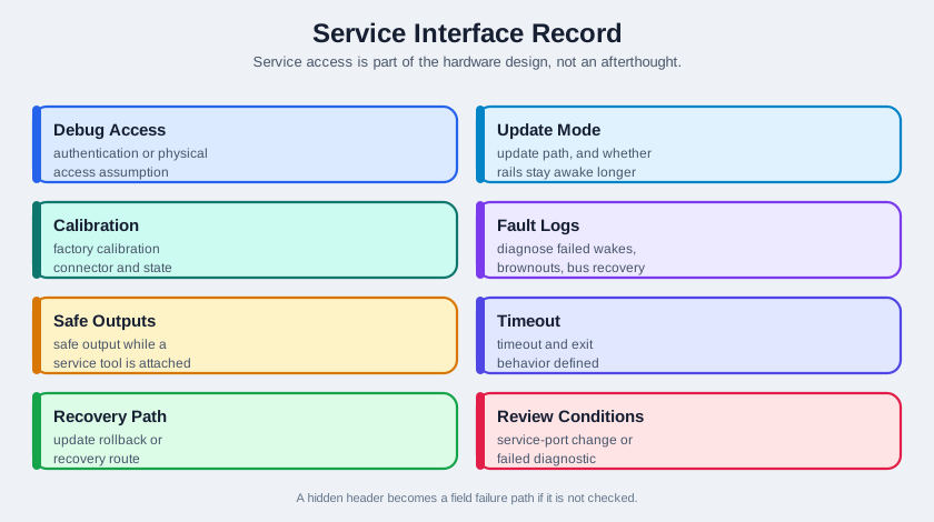
Service access is part of the hardware design. A hidden debug header, boot console, firmware update pin, or factory calibration connector can become a field failure path if it is not checked.
Check service interfaces for:
- authentication or physical access assumption;
- timeout and exit behavior;
- safe output behavior while a service tool is attached;
- update rollback or recovery path;
- logging needed to diagnose failed wakes, brownouts, and bus recovery;
- protection from miswiring, electrostatic events, and accidental back-feed;
- whether service mode keeps rails awake longer than normal operation.
20.14 Interface Resource Handoff Addendum
A hardware interface is only ready when the downstream firmware, message, service, and support resources preserve the same meaning. Keep a short handoff record for every interface that crosses a signal, driver, payload, API, or service boundary.
| Boundary | Handoff proof to keep |
|---|---|
| Signal to driver | Pin map, voltage domain, connector, timing, reset state, interrupt or wake behavior, bus capture, and error-reporting rule. |
| Driver to payload | Units, calibration state, timestamp, identity, quality flag, timeout, retry, stale-reading behavior, and schema version. |
| Payload to service | Topic or endpoint, authentication, authorization, duplicate handling, command expiry, retention, monitoring, and replay proof. |
| Resource to support | Datasheet or reference-design revision, driver/HAL version, SDK adapter limit, fixture or simulator coverage, release note, and service procedure. |
| Review condition | Pin change, sensor replacement, schema change, SDK update, service-port exposure, failed diagnostic, or field proof that contradicts the old interface record. |
This keeps GPIO, ADC, bus, UART, service-port, and API choices connected. A sample program proves a path only when its contract can be diagnosed, updated, and handed to the next owner.
20.15 Interface Decision Record
A good decision record is short, testable, and easy to review.
- Device role: Remote water valve node.
- Approved states: Boot, sleep, active sample, leak response, fault, service, update.
- Wake sources: Leak interrupt, scheduled timer, service button, watchdog.
- Critical boundaries: Leak input, valve driver, position feedback ADC, radio rail, service UART.
- Validation: Measure state draw at device input, wake latency, boot output default, stuck-bus recovery, service timeout, and fault output behavior.
- Review conditions: New actuator, longer external cable, new battery chemistry, service-port change, firmware update path change, or failed wake proof from the field.
20.16 Common Pitfalls
A wake input without a defined idle level can wake repeatedly, miss real events, or draw extra energy through a partly enabled input buffer. Define the idle level, pull method, debounce, edge, and retained rail.
Firmware can request sleep, but hardware decides what remains powered. Check sensor rails, pull-ups, wake sources, output drivers, clocks, and service ports before approving a sleep state.
Motors, relays, solenoids, valves, and long cables need driver stages and protection. A GPIO pin should command the driver; it should not be the power path for the load.
Outputs can move before firmware starts or after a reset. Use hardware defaults, pull behavior, and driver enables so actuators remain safe through boot, brownout, watchdog reset, and update mode.
I2C, SPI, and UART buses need ownership and recovery rules. A stuck device, wrong chip select, or boot console message can block a sensor path unless the decision record defines recovery behavior.
20.17 Knowledge Check
Key Concepts
- Power state: A named operating condition with entry rule, exit rule, supply draw, retained data, and output behavior.
- Wake source: A timer, pin, watchdog, radio event, service action, or external signal that can move the device out of a lower-power state.
- Retained state: Data or hardware context preserved while the rest of the device is paused or unpowered.
- GPIO: A configurable digital input or output used for simple signals, enables, interrupts, chip selects, and status lines.
- ADC: An analog-to-digital converter used when a physical value must be measured as a voltage within a defined range.
- PWM: A duty-pattern output used with a driver stage to control brightness, speed, heat, or actuator position.
- Level shifter: A circuit that makes logic signals compatible across different voltage domains.
- Open-drain bus: A bus style where devices pull a line low and an external pull-up sets the high level, common for I2C and shared alert lines.
- Back-feed: An unintended power path through a signal pin into an unpowered device or rail.
20.18 Prove State and Signal Together
If you only need the selection shortcut, this layer is enough: a low-power interface design is ready when every state has a wake rule, every signal has an owner, and the measured behavior matches the decision record.
For a valve node, state proof and signal proof have to be reviewed together. A low-power STM32L or nRF52-class controller may sleep well on its own, but the product still fails if the leak switch is powered from a rail that turns off, if the pull-up keeps drawing current through a wet connector, or if the valve driver briefly enables while reset pins float. The record should name the sleep rail, retained timer or GPIO wake source, valve-driver default, ADC reference, radio or modem burst, service UART timeout, and the test instrument used for current measurement.
The same record should say which interface is allowed to wake or move the product. GPIO inputs need idle level, debounce, interrupt edge, and ESD or surge assumptions. ADC feedback needs voltage range, divider current, source impedance, reference rail, and filter settling. PWM or enable outputs need a driver stage, flyback or transient protection, and a hardware default that keeps the valve safe before firmware starts. I2C, SPI, and UART links need ownership, voltage domain, recovery, and service-access rules.
State proof
Name boot, active, sleep, fault, service, and update states with entry rules, exit rules, retained data, safe outputs, and measured draw.
Signal proof
Map each GPIO, ADC, PWM, I2C, SPI, UART, wake line, actuator driver, and service port to one owner and one safe default.
Boundary proof
Check voltage range, pull behavior, debounce, level shifting, protection, back-feed, and recovery in the states that matter.
20.19 Valve Node Proof Record
For the remote water valve node, the decision should read like a field test plan. It should prove that the device can sleep, wake on a leak, close the valve safely, report health, and support service without creating a new electrical failure path.
Start the record with measured states rather than expected battery life. Measure sleep current with the leak input connected, pull network installed, sensor rail in its intended state, radio or modem fully off, and the service connector in its field configuration. Then measure the wake sequence: interrupt assertion, controller resume, sensor-rail enable, ADC feedback sample, valve-driver enable, actuator current, event write, and radio burst. Keep the oscilloscope capture, current trace, firmware build, board revision, ambient condition, and test temperature beside the table so the result can be repeated.
Next, map each boundary to a failure test. Pull the leak input high and low, short the sensor cable within the protected assumptions, reset the controller while the valve driver is attached, brown out during a flash write, hold I2C low, disconnect the radio module, and leave the service UART attached until timeout. The record is strong only when those tests return the device to a safe output state or a diagnosable fault state. Add pass limits for maximum wake latency, maximum sleep current, minimum ADC headroom, and service-session duration so later board revisions can be compared without guessing.
Wake path
Record the leak sensor rail, idle level, pull method, debounce, interrupt edge, retained state, wake latency, and first safe action after wake.
Output path
Show the valve driver default, enable timing, feedback range, brownout behavior, watchdog behavior, actuator current, and fault-state output rule.
Service path
Define the UART or tool boundary, authentication assumption, timeout, rail impact, logs, update recovery, and review conditions.
20.20 Why Sleep-Ready Boards Fail
Most failures come from a mismatch between the power state and the physical boundary. A signal can look correct during active testing and still fail when rails, pulls, clocks, service tools, or external modules change state.
The hidden problem is often a current path or ownership path that was invisible in the active demo. An I2C pull-up tied to the wrong rail can power a sleeping sensor through its data pin. A UART boot log can command or confuse a field modem before the application owns the port. A high-side driver can leak enough current to move a small actuator, while a low-side driver can leave the load referenced to an unsafe supply during reset. ADC dividers, status LEDs, sensor warm-up circuits, and protection networks all need the same state-by-state review as firmware.
- Retained rail mismatch: a wake source, pull-up, sensor, or timer is not powered in the sleep state that depends on it.
- Unsafe defaults: an actuator driver, chip select, enable pin, or PWM output moves during boot, brownout, reset, service, or update.
- Hidden current path: pull-ups, indicators, converters, external modules, or signal back-feed keep the device awake or drain the battery.
- Missing recovery: a stuck I2C device, noisy service cable, failed update, or watchdog reset has no tested path back to safe operation.
Recovery proof should include the path back from each fault, not only detection. For I2C, document whether firmware clocks the bus free, power-cycles the sensor rail, or disables the feature until service. For SPI, prove chip selects stay inactive during reset and that a partial flash or converter transfer does not corrupt the next sample. For UART, prove boot messages cannot enter the command stream, service sessions expire, and field tools cannot hold rails awake after the enclosure is closed. For ADC, prove the reference and divider settle before the sample is trusted.
20.21 Summary
Power management and device interfaces must be checked as one design surface. The state ledger explains when the device wakes, sleeps, faults, updates, and services. The interface map explains which component owns each signal and how that signal remains safe across voltage domains, boot, sleep, and fault behavior. The decision is complete only when measurements, wake behavior, boundary protection, and review conditions are recorded.
20.22 Key Takeaway
Power and interface decisions must connect electrical limits, sleep behavior, connectors, buses, and measurement proof before a hardware choice is trusted.
20.23 See Also
Hardware selection
- MCU vs MPU Selection - choosing controller-class or processor-class hardware from workload and lifecycle proof
- IoT System-on-Chip Architecture - internal SoC blocks, memory, clocks, power islands, and accelerators
Energy and sensing
- Energy-Aware Considerations - duty cycling, harvesting, and low-power design patterns
- Sensor Interfacing and Processing - sensor signal paths, sampling, conditioning, and processing
System architecture
- Edge-Fog Computing - deciding what runs on the device, gateway, and cloud path
20.24 What’s Next
| Direction | Chapter | Focus |
|---|---|---|
| Next | IoT System-on-Chip Architecture | SoC blocks, clocks, memory, and power islands |
| Back | MCU vs MPU Selection | Controller-class versus processor-class selection |
| Related | Energy-Aware Considerations | Low-power operation and duty cycling |