17 GPIO Output Stage Contracts
17.1 Start Simple
Imagine two devices sharing one logic line, but one tries to drive it HIGH while another drives it LOW. GPIO output stages define whether a pin actively drives both directions, only pulls LOW, or must rely on a resistor. Start by naming the output type, the pull-up value, and the condition that would create contention.
17.2 Learning Objectives
After this page, you should be able to:
- Distinguish push-pull outputs from open-drain/open-collector outputs at the transistor-stage level.
- Choose push-pull or open-drain behavior for SPI, PWM, chip-select, I2C, shared interrupt, and cross-rail interface lines.
- Explain how a pull-up resistor defines the HIGH level and why the resulting edge is slower than an actively driven HIGH.
- Identify bus-contention failure modes when multiple push-pull outputs are tied together.
- Review low-side load switching as the power-switching analogue of an open-drain output.
17.3 Why Transistor Choice Leads Here
Choosing the Right Transistor teaches how to pick BJTs, MOSFETs, ratings, heat margins, and protection for IoT load switches. This page narrows that selection into the output-stage contract that decides whether a pin actively drives both rails, only sinks current, or safely shares a line with other devices.
Use it when a GPIO line must be shared, a bus uses pull-ups, a level-shift depends on the pull-up rail, or a circuit review needs to prove that two output stages cannot fight each other.

Phoebe’s Why
This page’s own bus-contention warning says a “low-resistance path forms from Vcc through both output stages to GND” and “the logic level is ambiguous,” but it never puts a number on either claim. A sibling page in this module already derives the passive RC rise time an open-drain HIGH has to wait for. Contention is the opposite failure mode – two active push-pull outputs, both fully on – and a fully-on transistor is not an open switch or an ideal wire; it is a small, real resistance. Two of those resistances tied to opposite rails on the same node form nothing more exotic than a voltage divider, which is exactly why the node lands at an ambiguous voltage instead of a clean HIGH or LOW.
The Derivation
Model each fully-on output transistor as its on-resistance and apply Ohm’s law to the resulting loop:
\[I_{short} = \frac{V_{CC}}{R_{on,H}+R_{on,L}}\]
The contested node sits at the voltage divider between the two on-resistances, not at either rail:
\[V_{node} = V_{CC}\cdot\frac{R_{on,L}}{R_{on,H}+R_{on,L}}\]
Worked Numbers: Two Push-Pull Stages Fighting On A 3.3 V Rail
- Symmetric case, catalog-typical 30.0 Ω on-resistance for both stages: \(I_{short}=3.30/(30.0+30.0)=0.0550\) A \(=55.0\) mA, and \(V_{node}=3.30\times30.0/60.0=1.65\) V – dead center, neither a valid LOW nor a valid HIGH by the 0.80 V / 2.00 V thresholds derived elsewhere in this module. That is the numeric meaning of “ambiguous.”
- Against a normal load: \(55.0\) mA is \(3.67\times\) a catalog-typical \(15.0\) mA LED load and \(55.0\times\) a catalog-typical \(1.00\) mA I2C pull-up sink current – confirming this page’s own claim that contention current “can be much larger than the normal load current.”
- Against a rating: \(55.0\) mA already exceeds a catalog-typical \(40.0\) mA absolute-maximum per-pin current rating by \(1.38\times\) – the numeric version of this page’s “output transistors can be damaged.”
- Asymmetric case (unequal high-side/low-side strength, e.g. \(R_{on,H}=40.0\ \Omega\), \(R_{on,L}=20.0\ \Omega\)): \(I_{short}\) stays \(55.0\) mA (the sum in the denominator is unchanged), but \(V_{node}=3.30\times20.0/60.0=1.10\) V shifts toward the stronger (lower-resistance) side – contention current depends only on the total resistance in the loop, while which rail the ambiguous voltage leans toward depends on which side is stronger.
Overview: Two Ways an Output Stage Drives a Pin
The transistors at an output pin are wired in one of two ways, and the choice decides how the pin can be used. A push-pull stage has both a high-side device that pulls the pin up to Vcc and a low-side device that pulls it down to GND — exactly one on at a time, so it actively drives both a strong HIGH and a strong LOW. An open-drain (open-collector, for BJTs) stage has only the low-side transistor: it can pull the pin LOW or release it to high-impedance, and an external pull-up resistor is what makes the HIGH.
The easiest way to read a schematic is to ask who owns the wire in each state. A push-pull output owns the wire all the time: HIGH is an active source path and LOW is an active sink path. An open-drain output owns the wire only when it asserts LOW; when it releases, the pull-up resistor and the line capacitance decide how quickly the node rises. That difference is why push-pull suits private, point-to-point outputs, while open-drain suits shared or active-LOW signals.
Push-pull
Drives HIGH and LOW actively. Fast, strong both ways. The default for ordinary signals (SPI, PWM, chip-selects).
Open-drain
Sinks LOW only; HIGH is "released." Needs an external pull-up to define the HIGH level.
Wired-AND
Many open-drain outputs can share one line: any one pulling LOW wins, with no conflict.
Level flexibility
An open-drain line's pull-up can go to any allowed rail, setting the HIGH voltage independent of the chip's own Vcc.
For a private LED, chip-select, enable pin, or MOSFET gate, the board usually wants a decisive HIGH and LOW, so push-pull is the normal contract. For I2C, shared interrupt lines, reset aggregators, fault outputs, and presence-detect pins, the board often wants several devices to share one wire without coordinating who may talk first. Open-drain makes that possible because the only active assertion is LOW; all devices can release at the same time without fighting. The pull-up rail also becomes the logic-domain choice, so a 1.8 V sensor can sometimes signal a 3.3 V controller through a correctly rated open-drain line.
The naming can hide the physical rule. "Open" means the high-side path is missing, not that the pin is disconnected in every state. When the low-side transistor turns on, the pin is strongly connected to ground and can sink current. When it turns off, the pin becomes high impedance and needs the external circuit to define the voltage. If that external circuit is missing, the line is not a valid HIGH; it is just floating.
Overview Knowledge Check
Practitioner: Which Stage for Which Job
Use push-pull for ordinary fast digital signals that one driver owns: SPI clock and data, PWM to a gate driver, chip-select lines. It gives clean, quick edges in both directions.
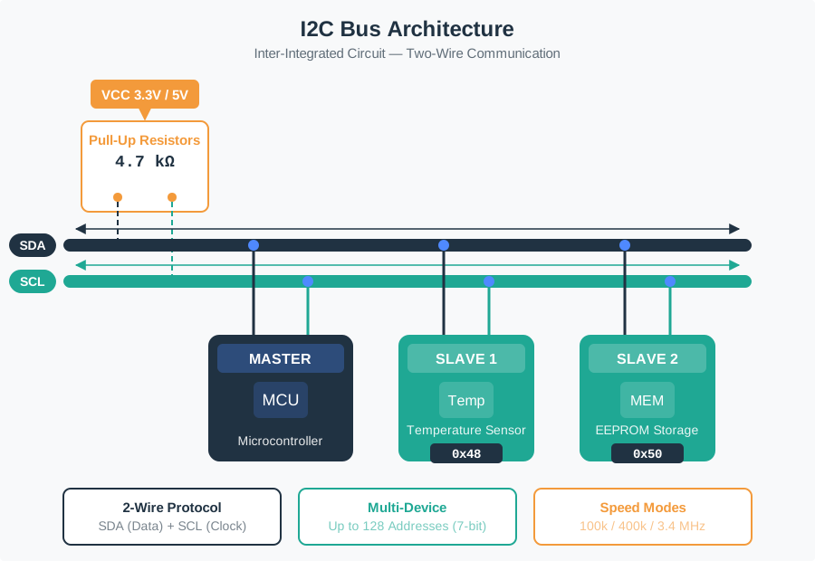
Use open-drain when a line must be shared or translated: I2C's SDA/SCL (many devices on two wires), a shared interrupt or "alert" line that several chips can assert, or an easy cross-rail interface where the pull-up sets the HIGH to 3.3 V or 5 V regardless of the chip's own supply. A transistor low-side load switch is the same idea in power form: the MOSFET pulls the load's return to ground while the load's other end sits at the supply.
Before choosing the stage, write the net's ownership rule in plain language. "The MCU is the only driver" points toward push-pull. "Any sensor may assert fault," "any peripheral may acknowledge," or "this line must idle HIGH until one participant pulls it LOW" points toward open-drain. The rule matters during reset and boot as much as during normal firmware. If two chips both default to push-pull output while their firmware is still starting, the schematic may be unsafe even if the application code later avoids simultaneous drive.
Worked example — switching a 12 V relay from a 3.3 V GPIO. Use a logic-level N-MOSFET as a low-side (open-drain-style) switch: GPIO to the gate, the relay coil between +12 V and the drain, source to ground, and a flyback diode across the coil to catch the turn-off spike. The GPIO only has to swing the gate; the drain switches the 12 V load the pin could never drive directly.
| Question in review | Push-pull answer | Open-drain answer |
|---|---|---|
| Who drives HIGH? | The output stage sources current through its high-side device. | The pull-up resistor raises the released line to its rail. |
| Can multiple devices share it? | Only with external arbitration that guarantees one active driver. | Yes, if all devices only sink LOW or release the line. |
| What sets edge speed? | Output-drive strength, load capacitance, trace length, and series damping. | Pull-up resistance times bus capacitance for the rising edge; sink strength for the falling edge. |
Pull-up sizing is the practical trap. A small resistor gives a faster rise but wastes more current whenever any device pulls LOW. A large resistor saves current but may rise too slowly or lose noise margin when leakage, long cables, ESD structures, or unpowered devices load the bus. The design review should name the rail, the resistor value, the expected line capacitance, the required rise time, and the worst-case LOW sink current. Without those checks, "open-drain" is only a schematic label, not a verified interface.
Low-side load switching follows the same contract with larger currents. The MOSFET drain node is released when the switch is off and is pulled near ground when it is on. The load sees supply voltage because its other side is tied to the positive rail, not because the microcontroller pin provides load power. That is why flyback protection, MOSFET current rating, logic-level gate drive, and a defined gate pull-down belong in the same checklist as the output-stage choice.
Practitioner Knowledge Check
Under the Hood: Bus Contention and the Passive-Edge Cost
The danger open-drain avoids is bus contention. Tie two push-pull outputs together and let one drive HIGH while the other drives LOW: you create a low-resistance path from Vcc through the first stage's high-side transistor and the second stage's low-side transistor to GND. Large current flows, the logic level is ambiguous, and the output transistors can be damaged. Open-drain outputs can only sink or release, so the worst case of "one pulling low, others released" simply gives a defined LOW — a wired-AND, never a fight.
That safety has a price. An open-drain HIGH is not driven; it happens only when the pull-up resistor charges the line capacitance, so the rising edge is a passive RC curve, slower than a push-pull's actively driven edge. This is exactly why I2C bus speed grades depend on the pull-up value and total bus capacitance: bigger capacitance or a weaker pull-up means a slower rise, which caps the usable clock frequency.
The contention current can be much larger than the normal load current because both output transistors are turned on hard. The exact value depends on the devices' on-resistances and current limiting, but the board-level conclusion does not: a push-pull net must have a single active owner at every instant. Firmware conventions such as "driver A speaks first" are not enough unless reset states, boot ROMs, sleep modes, programming headers, and fault paths also preserve that ownership rule.
Open-drain avoids that short because no participant ever sources a HIGH. If three devices share a line and one pulls LOW, current flows from the pull-up rail through the resistor into that one low-side transistor. The released devices see a LOW on their pins but do not drive against it. This is why active-LOW names such as ALERT_N, RESET_N, and INT_N are common: the asserted state is the one any participant can safely force.
| Failure mode | Electrical cause | Design countermeasure |
|---|---|---|
| Opposing outputs | One push-pull stage sources while another sinks on the same net. | Use one driver, tri-state arbitration, or convert the shared assertion to open-drain. |
| Slow released HIGH | Pull-up resistance and total bus capacitance form a long rise-time constant. | Choose a stronger pull-up within sink-current limits and reduce bus capacitance. |
| Wrong HIGH voltage | The pull-up rail exceeds a connected device's input tolerance. | Pull up only to a rail every attached device can tolerate, or add a proper level translator. |
A useful mental model is that a push-pull output is a two-throw switch connected to the rails, while an open-drain output is a one-throw switch to ground. The one-throw version is less powerful, but that limitation is what makes shared nets safe. In mixed-voltage IoT hardware, that limitation is often a feature: the bus HIGH belongs to the pull-up rail, while the active LOW is a current-sinking action that every tolerant device can observe.
Under-the-Hood Knowledge Check
17.4 Release Checklist
Before signing off a GPIO output-stage or shared-line design, verify that:
- Push-pull outputs are used only when one driver owns the line at a time.
- Open-drain/open-collector outputs have a pull-up resistor to an allowed rail and all connected devices tolerate that HIGH voltage.
- Pull-up value and line capacitance meet the required rise-time budget for I2C, interrupts, or other shared signals.
- No two push-pull outputs can drive opposite states on the same net during reset, boot, firmware updates, or fault handling.
- Low-side transistor switches include the same release-or-sink reasoning, plus flyback protection for inductive loads.
- Shared alert, reset, wake, or acknowledge lines document the wired-AND/active-LOW convention in schematics and firmware names.
17.5 See Also
- Choosing the Right Transistor: Return to transistor family, rating, heat, and protection selection.
- Edge Acquisition Architecture: Connect GPIO output behavior to real sensor-interface buses such as I2C, SPI, UART, and ADC.
- IoT Protocol Stack Architecture: Compare physical signal contracts with higher-layer protocol responsibilities.
- PCB Design: Carry pull-up and contention checks into schematic and layout review.
- Relay Interface: Connect low-side transistor switching to real inductive loads.
17.6 Next
After the output-stage contract is clear, continue with Electronics Summary and Resources to consolidate the module-level checklist.