Imagine a microcontroller pin trying to switch a motor, valve, or relay that needs far more current than the pin can supply. The transistor is the controlled switch between a small logic signal and a larger load path. Start with the load current, supply voltage, heat, switching speed, and the protection needed when the load turns off.
16.2 Learning Objectives
Apply a systematic decision framework to choose between BJT and MOSFET transistors for a given IoT application
Evaluate transistor specifications including voltage rating, current rating, power dissipation, and switching speed against project requirements
Distinguish between logic-level and standard MOSFETs and explain why logic-level devices are required for 3.3V/5V microcontroller circuits
Design a complete transistor switching circuit for a real-world IoT load, including flyback diode protection and proper gate drive
In 60 Seconds
Choosing the right transistor for your IoT project comes down to a few key decisions: BJT vs MOSFET (usually MOSFET wins for IoT), logic-level vs standard gate drive, and proper voltage/current/power ratings. For most microcontroller-driven loads, a logic-level N-channel MOSFET with a flyback diode handles 90% of use cases.
For Beginners: Choosing a Transistor
A transistor is like an electronic switch that lets a tiny signal from your microcontroller control a much bigger load, like a motor or a bright LED strip. There are two main types: BJTs (controlled by current, simpler for beginners) and MOSFETs (controlled by voltage, more efficient for most IoT projects). This guide helps you pick the right one for your project without getting lost in the thousands of options available.
16.3 Why This Chapter Matters
This is one of the most practical chapters in the whole book because it answers a frequent real-world question: how do I let a small microcontroller pin control something bigger safely.
Most beginner hardware damage happens when loads such as relays, motors, solenoids, and LED strips are connected as if GPIO pins were power supplies.
After this chapter, a student should be able to choose a reasonable transistor strategy instead of copying circuits without knowing why they work.
16.4 How To Use This Chapter
If you are a beginner, do not try to compare every transistor family at once. Start with the rule of thumb: logic-level N-channel MOSFETs solve most microcontroller load-switching problems.
Use the decision table first, then the application recommendations, and only then the detailed criteria.
Whenever a part number appears, connect it to a real task: relay driver, LED strip dimmer, motor switch, battery disconnect, or level shifter.
Chapter Roadmap
This chapter is a selection workflow, not a part-number catalog:
First you choose the transistor family from the load and power budget.
Then you check the common switching circuits and package trade-offs.
Next you verify voltage, current, heat, speed, and logic-level gate drive.
Finally you apply the rules to a garden valve, quizzes, and a bench design challenge.
Checkpoints recap the decision rules as you go, and anything titled “Deep dive” is optional on a first read.
16.5 Systematic Selection Process
16.5.1 Decision Framework: BJT vs MOSFET
Start with the family choice. The rest of the chapter only makes sense once you know whether you are paying for continuous base current or charging a MOSFET gate.
Start here to narrow down your choice between the two main transistor families:
Question
Choose BJT
Choose MOSFET
What’s your power budget?
Mains powered, continuous operation OK
Battery powered, need ultra-low power
What current are you switching?
< 500mA (BJT adequate)
> 500mA or need low losses
What’s your control signal?
Have current available (>1mA)
Limited current (<100µA GPIO)
How often does it switch?
Infrequent (<1 kHz)
High frequency (>10 kHz)
What’s your experience level?
Beginner (BJT simpler biasing)
Intermediate (MOSFET gate drive trickier)
Rule of Thumb: For modern IoT projects, MOSFET is usually the better choice due to voltage control (no base current drain), lower power losses (lower Rds(on)), and faster switching.
Deep dive: Putting Numbers to It
Consider switching a 2A DC motor with both BJT and MOSFET options. A power NPN BJT (TIP31C, rated for 3A) has \(V_{CE(sat)} = 0.5V\), giving power dissipation \(P_{BJT} = V_{CE(sat)} \times I_C = 0.5V \times 2A = 1W\). The BJT also requires base current: at \(I_C = 2A\), the TIP31C has \(\beta \approx 25\) (minimum guaranteed at high current), so \(I_B = 2A / 25 = 80mA\). This exceeds most GPIO limits, requiring a driver stage. For simplicity, assume a base driver provides adequate current. From a 5V driver: \(P_{base} = (5V - 0.7V) \times 80mA = 344mW\).
A logic-level N-channel MOSFET (IRLZ44N) has \(R_{ds(on)} = 28m\Omega\) (max) at \(V_{gs} = 5V\). Power dissipation: \(P_{MOSFET} = I_D^2 \times R_{ds(on)} = (2A)^2 \times 0.028\Omega = 0.112W\). Gate current is essentially zero (<1µA). Total MOSFET losses: 0.112W vs. BJT losses: 1.344W (1W conduction + 344mW base drive) – the MOSFET is 12x more efficient. For battery-powered IoT nodes operating 24/7, this translates to months of extended battery life.
A switch transistor is judged by how much energy it wastes while forcing charge carriers through silicon. A BJT switch needs a steady base-current stream to flood the base region, then it still leaves a small collector-emitter voltage drop while saturated. A MOSFET gate is different: the GPIO builds an electric field across an insulated gate. Once that field inverts the channel, the drain-source path behaves like a small resistor. That is why the useful MOSFET datasheet line is not just \(V_{GS(th)}\); it is \(R_{DS(on)}\) at the gate voltage the microcontroller can actually supply.
The Derivation
For a BJT in its active region, collector current is set by base current:
\[I_C = \beta I_B\]
To use it as a switch, the base is overdriven until the device saturates, so the remaining voltage drop dissipates heat:
\[P_{CE} = V_{CE(sat)} I_C\]
The driver also spends power feeding the base-emitter junction:
\[P_{base} = (V_{drive} - V_{BE}) I_B\]
For a MOSFET, the gate field creates the channel only after threshold:
\[V_{GS} > V_{GS(th)}\]
Full enhancement is the lower-resistance condition the datasheet certifies:
\[V_{DS} = I_D R_{DS(on)}\]
So the on-state heat is
\[P_{MOSFET} = I_D V_{DS}\]
\[P_{MOSFET} = I_D^2 R_{DS(on)}\]
The package turns that electrical loss into junction temperature:
\[\Delta T_J = P\,\theta_{JA}\]
Worked Numbers: This Motor Switch
BJT base current:\(I_B = I_C/\beta\)\(= 2.00/25\)\(= 0.0800\) A \(= 80.0\) mA, already beyond a typical GPIO pin.
BJT heat path:\(P_{CE} = 0.5 \times 2.00\)\(= 1.00\) W, and \(P_{base} = (5.00 - 0.700)\times0.0800\)\(= 0.344\) W, so \(P_{total}=1.34\) W.
MOSFET channel loss:\(P = I_D^2R_{DS(on)}\)\(= (2.00)^2\times0.0280\)\(= 0.112\) W for the IRLZ44N at \(V_{GS}=5.00\) V.
Efficiency check:\(1.344/0.112\)\(= 12.0\), matching the chapter’s 12x advantage.
Thermal meaning: with a TO-220 no-heatsink value near \(62\) deg-C/W, the MOSFET rise is \(0.112\times62\)\(= 6.94\) deg-C; the BJT case would be \(1.344\times62\)\(= 83.3\) deg-C before any outdoor ambient margin.
The selection rule follows directly: choose the transistor whose controlled region matches the load. For a microcontroller motor switch, a logic-level MOSFET whose \(R_{DS(on)}\) is specified at the real gate voltage turns the same 2 A load into a small thermal problem instead of a driver-current and heat problem.
Checkpoint: Family Choice
You now know:
Battery-powered IoT designs usually favor MOSFETs because the gate draws essentially zero steady current.
A 2A load can push a TIP31C BJT into an 80mA base-current problem, while the IRLZ44N example dissipates 0.112W.
The decision table is a filter: power budget, current, control signal, switching rate, and experience level all matter.
16.5.2 Transistor Switching Circuits for IoT
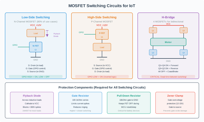
Once the transistor family is narrowed, choose where the switch sits in the load path. Low-side, high-side, H-bridge, and flyback protection solve different wiring problems.
The most common transistor configurations you’ll encounter in IoT hardware design:
Figure 16.1: MOSFET Switching Circuits: Low-Side, High-Side, and H-Bridge Configurations
L298N module (integrated, no external gate drivers needed)
5V→3.3V level shifter
BSS138 (N-channel SOT-23)
50V, 200mA, Rds(on)=3.5Ω
Standard for bidirectional I2C/SPI shifting
2N7000 (through-hole version)
Signal amplifier (audio)
2N3904 (NPN) + 2N3906 (PNP)
Complementary pair for push-pull
Low noise, good for small-signal amplification
BC547/BC557 pair
SMD vs Through-Hole Trade-Offs:
Through-hole (TO-92, TO-220): Easier for beginners, hand-solderable, good heat dissipation (TO-220 with heatsink)
SMD (SOT-23, SOT-223, DPAK): Compact for production, cheaper in volume, harder to solder by hand
16.5.4 Detailed Selection Criteria
The recommendation table gives a starting part. The detailed criteria below are the safety checks that decide whether that part survives in the actual product.
When the simple recommendation table doesn’t fit your needs, use these detailed criteria:
Voltage Rating (V_CE, V_DS)
What to check: Maximum voltage between collector-emitter (BJT) or drain-source (MOSFET)
Selection rule: Choose transistor with voltage rating ≥ 2× your supply voltage for safety margin
Switching losses: At high frequencies, switching losses dominate. Use MOSFETs with low gate charge (Q_g) for efficiency.
Common mistake: Using slow Darlington (TIP120) for 20 kHz PWM → overheating, poor efficiency
Logic-Level MOSFET Drive
Critical MOSFET selection criterion often overlooked by beginners!
Standard MOSFETs:
Need V_GS = 10-12V to achieve the specified low Rds(on)
IRF540N datasheet: Rds(on) = 44mΩ @ V_GS = 10V
With 5V gate drive: Rds(on) = ~200mΩ (4.5× higher → 4.5× more heat!)
Logic-Level MOSFETs:
Specified for low Rds(on) at V_GS = 4.5-5V; for 3.3V GPIO, prefer parts with Rds(on) specified at 2.5-3.3V
IRLZ44N datasheet: Rds(on) = 28mΩ max @ V_GS = 5V (OK for 5V gate drive; check curves before relying on 3.3V)
Note the “L” in IRLZ44N → Logic-level
Selection rule:
3.3V/5V microcontroller: MUST use a logic-level MOSFET, and must verify Rds(on) at the gate voltage you can actually provide; V_GS(th) alone is not enough
12V+ gate driver: Can use standard MOSFET (often cheaper, lower Rds(on))
Common beginner mistake: “My IRF540N gets really hot even though it’s rated for 33A and I’m only switching 2A” → Using standard MOSFET with 5V gate drive! Solution: Replace with IRLZ44N (logic-level version)
Checkpoint: Ratings and Gate Drive
You now know:
Voltage rating should be at least 2x the supply, and current rating should be about 2-3x the load current.
Power loss has to fit the package: a TO-92 example can fail near 0.15W at 60 deg-C, while MOSFET loss uses I^2 x Rds(on).
For 3.3V or 5V GPIO, “logic-level” means checking Rds(on) at the gate voltage you can actually provide.
16.5.6 Garden Irrigation Transistor
Now apply the checklist to a real actuator. The valve example ties together load current, flyback protection, GPIO limits, outdoor temperature, and battery life.
Requirements:
Control 12V solenoid valve (opening/closing water flow)
Solenoid coil: 12V, 50mA nominal, 200mA inrush current
Controlled by ESP32 GPIO (3.3V, 12mA max)
Battery powered (need low quiescent current)
Outdoor deployment (temperature: -10°C to +60°C)
Decision Process:
Step 1: BJT or MOSFET? - Battery powered → prefer MOSFET (zero gate current) - Load: 200mA → either works, but MOSFET more efficient - Choice: MOSFET
Step 2: Voltage rating? - Solenoid: 12V → need ≥24V rating for safety (2x rule) - With flyback diode, inductive spikes are clamped to ~12.7V - Requirement: V_DS ≥ 24V (flyback diode limits spike voltage)
Step 4: Logic-level or standard? - ESP32 GPIO: 3.3V → MUST be logic-level - Need logic-level behavior and low Rds(on) at the available gate drive; for ESP32, prefer datasheet data at 2.5-3.3V or a dedicated gate driver - Requirement: Logic-level MOSFET verified at the actual GPIO voltage
Step 5: Package and thermal? - P_dissipation = I² × Rds(on) = (0.2)² × 0.03Ω = 1.2mW - Negligible heat → no heatsink needed - Requirement: Any package (TO-92, SOT-23)
Final Selection: 2N7002 (N-channel MOSFET, SOT-23) or IRLML2502 for more margin - V_DS: 60V (OK: safe for 12V + inductive spikes) - I_D: 115mA continuous (2N7002, SOT-23 package limited; OK for 50mA nominal because the 200mA inrush is brief) - V_GS(th): 1.0-2.5V typical (OK: reliably on at 3.3V) - Package: SOT-23 (OK: compact, easy to solder) - Cost: $0.05 (OK: very cheap) - Rds(on): 2.0Ω @ V_GS=2.5V → P = (0.05A)^2 x 2.0 = 5mW nominal (OK: negligible losses)
Note: The popular 2N7000 (TO-92, 200mA) is also viable here since nominal current is only 50mA, but the 2N7002 offers better margin and a smaller footprint.
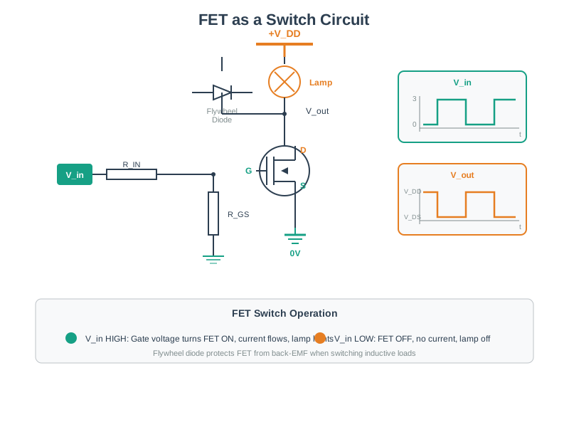
Additional Protection: Add 1N4007 flyback diode across solenoid coil (cathode to +12V, anode to drain) to protect MOSFET from inductive kickback when solenoid turns OFF.
Wiring map:
Connection
Where It Goes
Why
ESP32 GPIO
1kΩ series resistor, then MOSFET gate
Limits the brief gate-charging current
MOSFET source
GND
Completes the low-side switch path
MOSFET drain
Solenoid negative side
Lets the MOSFET pull the solenoid to ground when ON
Solenoid positive side
+12V supply
Provides load power
Flyback diode cathode
+12V side of solenoid
Blocks current during normal operation
Flyback diode anode
MOSFET drain side of solenoid
Safely recirculates coil current when the MOSFET turns OFF
Why NOT alternatives:
BJT (2N3904): Needs base current (~2mA), wastes battery power during sleep cycles
IRF540N: Standard gate (not logic-level), won’t fully turn on with 3.3V
Relay: 50mA coil current wasteful for battery, mechanical wear, slower
LoRaWAN Valve Transistor
Scenario: You’re designing a remote irrigation valve controller powered by LoRaWAN. The 12V solenoid valve coil draws 300mA nominal, with 800mA inrush current when first energized. The system runs on 4× AA batteries (6V total) with a boost converter to 12V. The LoRa module (RFM95) GPIO output is 3.3V at 12mA max. Battery life target is 2 years with 10 valve actuations per day, each lasting 30 seconds.
Specs: 55V V_DS (ample margin with flyback diode clamping spikes to ~12.7V), 47A I_D, 28mΩ Rds(on) max @ 5V, TO-220 package
Cost: ~$0.80 in single quantities, $0.35 in 100+ quantities
Flyback diode: 1N4007 (1000V, 1A) across valve coil – essential for clamping inductive voltage spikes
Gate resistor: 10kΩ pull-down from gate to ground (keeps MOSFET OFF when RFM95 is sleeping)
Gate series resistor: 100Ω between GPIO and gate (limits current spikes)
Wiring map:
Connection
Where It Goes
Why
RFM95 GPIO (3.3V)
100Ω series resistor, then IRLZ44N gate
Controls the valve while limiting gate current spikes
Gate pull-down
10kΩ from gate to GND
Keeps the valve OFF while the radio module boots or sleeps
IRLZ44N source
GND
Low-side switching reference
IRLZ44N drain
Solenoid valve negative side
MOSFET switches the valve current
Solenoid valve positive side
+12V supply
Provides valve power
1N4007 flyback diode
Cathode to +12V, anode to MOSFET drain
Protects the MOSFET from inductive kickback
Key Lessons:
Inductive loads always need flyback diodes - without it, inductive kickback can generate 300V+ spikes destroying the MOSFET
Logic-level is non-negotiable for 3.3V systems - standard MOSFETs won’t fully turn on, causing excessive heat
Check Rds(on) at YOUR gate voltage - datasheets often spec at 10V, but you’re using 3.3V
Pull-down resistors prevent float-induced turn-on - critical for systems with sleep modes
Power dissipation is usually negligible - the 3.15mW loss is only 0.088% of the 3.6W valve power (12V x 300mA)
Real-World Validation: After deployment, measure the MOSFET temperature rise. With 3mW dissipation, temperature rise will be approximately: - Thermal resistance junction-to-ambient (TO-220, no heatsink): ~62°C/W - Temperature rise: 3mW × 62°C/W = 0.19°C - Essentially unmeasurable - confirms calculations were correct
16.6 Deep dive: Re-deriving the chapter’s numbers
Check
Calculation
Result
BJT base current
2 A / 25 = 0.080 A
80 mA, beyond typical GPIO drive
BJT loss including drive
(0.5 V x 2 A) + ((5 V - 0.7 V) x 0.080 A) = 1.344 W
Real heat plus driver power
MOSFET conduction loss
(2 A)^2 x 0.028 ohm = 0.112 W
1.344 / 0.112 = 12.0x lower loss
Solenoid inrush heat screen
(0.2 A)^2 x 0.030 ohm = 0.0012 W
1.2 mW, so package heat is not the limiting factor
Valve daily MOSFET loss
(0.3 A)^2 x 0.035 ohm = 0.00315 W; 0.00315 W x (10 x 30 / 3600) h = 0.0002625 Wh/day
0.2625 mWh/day
Two-year battery cost
0.0002625 Wh/day x 730 / 6 V = 0.03194 Ah
31.94 mAh, or 31.94 / 2500 = 1.28% of one AA string capacity
Package temperature rise
0.00315 W x 62 deg-C/W = 0.1953 deg-C
Effectively unmeasurable, matching the validation rule
The design implication is that the MOSFET is not just more efficient in the calculator. It removes an impossible GPIO base-current demand, leaves thermal headroom for outdoor temperatures, and keeps the battery penalty small enough that the valve coil energy dominates the lifetime budget.
Checkpoint: Applied Valve Design
You now know:
A 12V solenoid needs flyback protection, and the 2x voltage-rating rule turns that into at least a 24V transistor check.
The valve example separates 200mA inrush from 50mA nominal current, then verifies logic-level drive from a 3.3V ESP32 GPIO.
In the LoRaWAN valve case, MOSFET loss is small: 3.15mW, about 31.94mAh over 730 days, or 1.28% of the AA string capacity.
16.7 Chapter Summary
The worked examples have done the arithmetic; the summary turns those checks into a reusable field procedure.
Transistor selection for IoT follows a systematic process: start with the BJT vs MOSFET decision (MOSFETs win for most battery-powered applications due to zero gate current and lower conduction losses), then verify four critical specifications against your requirements.
The four key selection criteria are: (1) voltage rating at least 2x your supply voltage to handle transients, (2) current rating at least 2-3x your load current for thermal margin, (3) power dissipation within the package limits (P = I^2 x Rds(on) for MOSFETs, P = Vce(sat) x Ic for BJTs), and (4) logic-level gate compatibility if driven directly from a 3.3V or 5V microcontroller GPIO.
Logic-level MOSFETs are essential for microcontroller-driven circuits. Standard MOSFETs require Vgs = 10V to achieve their rated Rds(on), leading to excessive heating when driven from 3.3V/5V GPIOs. Always check Rds(on) at your actual gate voltage in the datasheet, not the headline specification.
Protection circuits are non-negotiable for inductive loads: flyback diodes across relay coils, solenoids, and motors prevent destructive voltage spikes when the transistor switches off. Gate pull-down resistors keep MOSFETs off during microcontroller reset or sleep states.
Quiz 3: Comprehensive Review
For Kids: Meet the Sensor Squad!
The Sensor Squad goes shopping for the perfect transistor!
Max the Microcontroller had a mission: he needed to control a small water valve for a smart garden. “But I can only push with 3.3 volts and 12 milliamps,” Max said. “The valve needs 12 volts and 100 milliamps! I need a transistor helper.”
The Sensor Squad went to the Electronics Store, where they found LOTS of transistors. “There are two main types,” explained Sammy the Sensor. “BJTs and MOSFETs.”
“A BJT is like a faucet,” said Lila the LED. “You have to keep pushing the handle (sending current to the base) to keep it open. If you let go, it closes.” “A MOSFET is like a light switch,” added Bella the Battery. “You just flip it (send voltage to the gate) and it stays on without you pushing. Much better for saving my energy!”
Max picked up a MOSFET called the 2N7000. “Let’s check if this one works for us. Voltage rating: 60V – our valve is 12V, so we have plenty of safety margin. Current rating: 200mA – that’s double what our valve needs, giving us a safety margin. And it’s logic-level, which means my 3.3 volt signal can turn it on. Perfect!”
“Don’t forget the flyback diode!” warned Sammy. “The valve has a coil inside that stores energy in a magnetic field. When Max turns it off, that energy has to go somewhere, and it creates a huge voltage spike that could destroy the transistor!” They added a 1N4007 diode across the valve to protect everything.
“So choosing a transistor is like choosing the right tool for the job,” concluded Max. “Check the voltage, check the current, make sure it works with your signal level, and always add protection for valves and motors!”
16.7.1 Key Words for Kids
Word
What It Means
MOSFET
A type of transistor that works like a light switch (voltage controlled)
BJT
A type of transistor that works like a faucet (current controlled)
Logic-Level
A MOSFET that can be turned on by a microcontroller’s small voltage
Flyback Diode
A protector that absorbs voltage spikes from motors and pumps
Voltage Rating
The maximum voltage a transistor can handle safely
Current Rating
The maximum current a transistor can carry safely
16.8 MOSFET Gate Drive Basics
The earlier sections treat gate drive as a selection rule. This optional section explains the device behavior behind that rule.
N-Channel MOSFET Operation Step by Step
The big picture: A MOSFET acts as a voltage-controlled switch where applying voltage to the gate terminal creates a conductive channel between drain and source, allowing current to flow with very low resistance (typically 0.01-0.1Ω for power MOSFETs).
Step-by-step breakdown:
OFF State (Vgs = 0V): No gate voltage applied, P-type body region blocks current flow between N-type drain and source with >1MΩ resistance, leakage current <1µA - Real example: IRLZ44N with 12V across drain-source passes only 0.25µA when gate is grounded
Threshold (Vgs = 2V): Gate voltage reaches threshold, creating thin conductive channel of electrons at oxide interface, resistance drops to ~10Ω, enabling milliamp-level currents - Real example: At Vgs = 2V, IRLZ44N conducts 100mA with 1V drop across channel
Fully Enhanced (Vgs = 5V): Strong gate electric field inverts surface from P-type to N-type, forming wide low-resistance channel (~50nm deep), Rds(on) = 0.028 ohm max enabling 47A rating - Real example: At Vgs = 5V, IRLZ44N passes 10A with only 0.28V drop, dissipating 2.8W heat
Why this matters: Gate threshold voltage (Vgs(th)) determines microcontroller compatibility. Standard MOSFETs need 10V, logic-level MOSFETs work with 3.3-5V GPIO. Using wrong type causes partial turn-on, high resistance, and excessive heating.
16.9 Concept Check: MOSFET Selection
Test your transistor selection skills:
16.10 Concept Relationships
Transistor selection connects throughout IoT hardware design:
After the quizzes, turn the rules back into a circuit. This relay exercise checks whether you can choose the part, size the resistor, and place the diode without copying blindly.
Challenge: Design a Load Switching Circuit
Objective: Select proper transistor, calculate component values, and draw complete circuit for microcontroller-controlled relay.
Specification:
Relay coil: 5V, 70mA, 100Ω coil resistance
Microcontroller: Arduino Uno (5V GPIO, 40mA max)
Requirement: Simple, low-cost circuit
Steps:
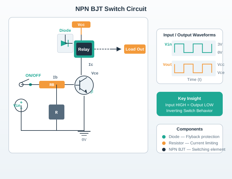
Choose transistor type: BJT vs MOSFET? (70mA suggests BJT acceptable)
Calculate base resistor for BJT OR gate resistor for MOSFET
Add flyback diode protection (inductive load!)
Draw complete circuit with all component values
Solution:
Item
Selection
Reason
Transistor
2N2222 NPN BJT
40V, 600mA rating gives comfortable margin for a 70mA relay coil
Base resistor
4.7kΩ from Arduino Pin 9 to base
Gives about 0.91mA base current, enough overdrive for reliable saturation
Flyback diode
1N4007 across relay coil
Cathode/stripe to +5V, anode to transistor collector
Wiring map:
Arduino / Component Node
Connects To
Arduino Pin 9
4.7kΩ resistor, then 2N2222 base
2N2222 collector
Relay coil negative side
Relay coil positive side
+5V supply
2N2222 emitter
GND
1N4007 diode
Across the relay coil, stripe/cathode to +5V
Expected Observation: Relay clicks ON when GPIO HIGH, OFF when LOW. MOSFET alternative (2N7000) would use 10k-ohm pull-down + 100-ohm gate resistor instead, drawing <1uA vs BJT’s 0.9mA base current.
16.11.1 BJT Base Resistor Calculator
Use this calculator to find the base resistor value for any BJT switching circuit.
Show code
viewof bjt_vcc = Inputs.range([3.3,24], {value:5,step:0.1,label:"Supply Voltage Vcc (V)"})viewof bjt_ic_load = Inputs.range([1,5000], {value:70,step:1,label:"Load Current Ic (mA)"})viewof bjt_beta_val = Inputs.range([20,500], {value:100,step:10,label:"Transistor Beta (hFE)"})viewof bjt_overdrive = Inputs.range([1.0,5.0], {value:2.0,step:0.1,label:"Overdrive Factor (typ. 2x)"})
Show code
bjt_vbe =0.7bjt_ib_min = (bjt_ic_load /1000) / bjt_beta_valbjt_ib_design = bjt_ib_min * bjt_overdrivebjt_rb_calc = (bjt_vcc - bjt_vbe) / bjt_ib_designbjt_standard_values = [100,120,150,180,220,270,330,390,470,560,680,820,1000,1200,1500,1800,2200,2700,3300,3900,4700,5600,6800,8200,10000,12000,15000,18000,22000,27000,33000,39000,47000]bjt_rb_standard = bjt_standard_values.reduce((prev, curr) =>Math.abs(curr - bjt_rb_calc) <Math.abs(prev - bjt_rb_calc) ? curr : prev)bjt_ib_actual = (bjt_vcc - bjt_vbe) / bjt_rb_standardbjt_pb_actual = (bjt_vcc - bjt_vbe) * bjt_ib_actualhtml`<div style="background:#f8f9fa; border:1px solid #dee2e6; border-radius:8px; padding:16px; margin:8px 0; font-family:Arial,sans-serif;"><h4 class="depth-l1" style="margin-top:0; color:#2C3E50;">BJT Base Resistor Calculator</h4><table style="width:100%; border-collapse:collapse;"><tr style="background:#E67E22; color:white;"><th style="padding:8px; text-align:left;">Parameter</th><th style="padding:8px; text-align:right;">Value</th></tr><tr><td style="padding:6px; border-bottom:1px solid #ddd;">Minimum Base Current (Ib = Ic / beta)</td><td style="padding:6px; text-align:right; border-bottom:1px solid #ddd;">${(bjt_ib_min *1000).toFixed(3)} mA</td></tr><tr><td style="padding:6px; border-bottom:1px solid #ddd;">Design Base Current (with ${bjt_overdrive}x overdrive)</td><td style="padding:6px; text-align:right; border-bottom:1px solid #ddd;">${(bjt_ib_design *1000).toFixed(3)} mA</td></tr><tr><td style="padding:6px; border-bottom:1px solid #ddd;">Calculated Rb = (Vcc - 0.7V) / Ib</td><td style="padding:6px; text-align:right; border-bottom:1px solid #ddd;">${bjt_rb_calc.toFixed(0)} ohm</td></tr><tr style="background:#E8F5E9; font-weight:bold;"><td style="padding:6px; border-bottom:1px solid #ddd;">Nearest Standard Value</td><td style="padding:6px; text-align:right; border-bottom:1px solid #ddd;">${bjt_rb_standard >=1000? (bjt_rb_standard/1000).toFixed(1) +' k': bjt_rb_standard} ohm</td></tr><tr><td style="padding:6px; border-bottom:1px solid #ddd;">Actual Base Current (with standard Rb)</td><td style="padding:6px; text-align:right; border-bottom:1px solid #ddd;">${(bjt_ib_actual *1000).toFixed(3)} mA</td></tr><tr><td style="padding:6px; border-bottom:1px solid #ddd;">Base Resistor Power Dissipation</td><td style="padding:6px; text-align:right; border-bottom:1px solid #ddd;">${(bjt_pb_actual *1000).toFixed(2)} mW</td></tr>${bjt_ib_actual *1000>20?`<tr style="background:#FFEBEE;"><td style="padding:6px; font-weight:bold; color:#E74C3C;" colspan="2">Warning: Base current (${(bjt_ib_actual *1000).toFixed(1)} mA) exceeds typical GPIO limit (20mA). Use a driver stage or switch to MOSFET.</td></tr>`:''}</table><p style="margin-top:8px; font-size:0.9em; color:#666;">Overdrive factor > 1 ensures the BJT is driven firmly into saturation, even with beta variation across temperature and manufacturing.</p></div>`
GPIO Output Stage Contracts - Deep dive into push-pull versus open-drain outputs, shared bus lines, and contention risks
Quiz 4: Match the Terms
Match each transistor term or component to its correct role or definition.
Quiz 5: Order the Steps
Arrange the following steps in the correct order to select and design a transistor switch for an IoT actuator.
Label the Diagram
16.13 Continue: GPIO Output Stage Contracts
The main chapter above stays focused on selecting BJTs, MOSFETs, ratings, gate drive, heat, and protection for IoT loads. For the deeper design contract behind push-pull versus open-drain outputs, pull-up-defined HIGH levels, shared I2C-style lines, and bus-contention failure modes, continue to GPIO Output Stage Contracts.
Choose the transistor from the load backward. Current, voltage, switching speed, high-side or low-side placement, GPIO drive level, heat, and protection needs determine whether a BJT, logic-level MOSFET, or driver IC is appropriate.

 Checkpoint: Family Choice