7 Op-Amp Sensor Front-End Contracts
7.1 Start Simple
Imagine a weak sensor voltage that changes when temperature, light, or pressure changes. The op-amp is useful only if it presents the right input load, produces a voltage the ADC can read, and stays inside its rails and bandwidth. Start with the sensor range, the ADC range, and the one gain or buffer job the front end must prove.
7.2 Learning Objectives
After this page, you should be able to:
- Use the negative-feedback op-amp golden rules without applying them outside their valid range.
- Choose a buffer, non-inverting amplifier, inverting amplifier, or comparator for a sensor front-end job.
- Explain how a unity-gain follower prevents voltage-divider loading errors.
- Check output swing, input common-mode range, and supply rails before trusting an amplified signal.
- Estimate closed-loop bandwidth from gain-bandwidth product and selected gain.
7.3 Why Op-Amps Follow Circuits
Electricity in Real IoT Circuits shows how passive components create divider outputs, pull-ups, filters, LED limits, and battery budgets. This page takes the next step: what happens when a passive node must drive a real load, feed an ADC, or produce a clean threshold decision.
Use it when a divider output sags, a sensor signal is too small for the ADC range, a noisy threshold needs hysteresis, or an amplifier data sheet must be translated into usable gain and bandwidth.

Phoebe’s Why
Further down this page, closed-loop bandwidth is given as approximately GBW divided by gain, as if that were a rule to memorize. It falls straight out of the two golden rules once the op-amp’s own open-loop gain is allowed to roll off with frequency, the way every real op-amp’s does. A real op-amp is not infinite gain at every frequency; it is huge gain at DC that falls at a steady rate past a very low corner. Feedback trades some of that huge DC gain for bandwidth, and exactly how much bandwidth comes back for a chosen closed-loop gain is fixed by the derivation below.
The Derivation
Single-pole open-loop model, with corner \(f_c\) and DC gain \(A_0\):
\[A_{OL}(f) = \frac{A_0}{1 + j f/f_c}\]
For \(f \gg f_c\): \(|A_{OL}(f)| \approx A_0 f_c / f = \mathrm{GBW}/f\), where \(\mathrm{GBW} = A_0 f_c\) is the frequency at which \(|A_{OL}| = 1\).
With feedback factor \(\beta = R_g/(R_f+R_g)\), this page’s own golden rules give ideal closed-loop gain \(A_v = 1/\beta = 1 + R_f/R_g\), and
\[A_{CL}(f) = \frac{A_{OL}(f)}{1 + \beta A_{OL}(f)}\]
The \(-3\) dB point is where \(\beta |A_{OL}(f)| = 1\):
\[\beta \cdot \frac{\mathrm{GBW}}{f_{-3dB}} = 1 \quad\Longrightarrow\quad f_{-3dB} = \frac{\mathrm{GBW}}{A_v}\]
Worked Numbers: This Page’s Own Gain-100 Example
- This page’s own example: a 1 MHz-GBW op-amp at gain 100 gives \(f_{-3dB} = (1\times10^6)/100 = 1.00\times10^4\) Hz \(= 10.0\) kHz – this page’s own figure, exact.
- The same 1 MHz-GBW part used as this page’s own unity-gain buffer (\(A_v = 1\)) keeps essentially the whole GBW as bandwidth: \(f_{-3dB} = (1\times10^6)/1 = 1.00\) MHz – \(100\times\) more bandwidth than the gain-100 stage, from the same silicon.
- Noise gain equals this same \(A_v = 1+R_f/R_g\) for the non-inverting stage this page derives, so the identical GBW/gain ceiling that limits signal bandwidth also limits how much input-referred offset and noise the stage amplifies – a high-gain front end is not just slower, it is noisier in exactly the ratio its bandwidth shrank.
7.4 Two Rules for Op-Amps
An operational amplifier (op-amp) is a high-gain differential amplifier — it amplifies the difference between its + and − inputs. An amplifier is the active opposite of an attenuator: it takes energy from a supply and uses it to produce a larger output signal while preserving the input shape as much as the circuit allows. Depending on the job, that gain may be expressed as voltage gain, current gain, transconductance, or transresistance, but the design question is always the same: what signal is being made larger, where does the extra energy come from, and what limit will distort it first? A practical op-amp is a DC-coupled integrated circuit built from many transistors, with differential inputs, a single output, high open-loop gain, and enough availability that it becomes the cheap, reusable building block for buffers, gain stages, comparators, and sensor front ends.
When it is wrapped in negative feedback (output fed back to the − input), two “golden rules” hold and let you analyze the standard circuits by inspection:
- No input current: the inputs are near-infinite impedance and draw essentially nothing.
- Virtual short: the output does whatever it takes to force
V+ = V−(valid only with negative feedback and an unsaturated output).
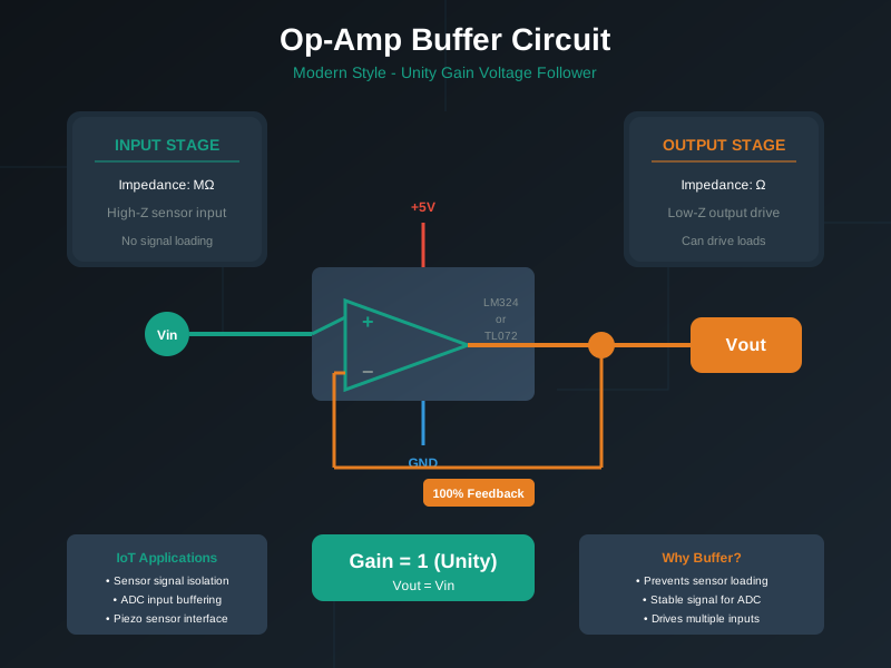
That contract language matters. A buffer promises voltage isolation, a non-inverting amplifier promises a scaled same-polarity signal, an inverting amplifier promises a scaled opposite-polarity signal around its reference node, and a comparator promises a rail-level decision. Before solving any resistor equation, name the job, the source impedance, the load or ADC input, the required gain, the allowed output range, and whether the output must remain analog.
Specification matching starts with the two voltages you actually have: the board-side signal level and the project-side requirement. If a 1.8 V GPIO path must drive a higher analog threshold or ADC span, the amplifier is sized around that ratio instead of around a convenient part. For a non-inverting stage, the golden rules give V+ = V− and essentially zero input current, so the feedback divider current is set by the two resistors and the closed-loop gain becomes Av = 1 + Rf/Rg. Choose the gain target, select practical resistor values, then check the op-amp supply rails and output swing before building the stage.
A package diagram is part of that contract. An NTE987-style quad op-amp does not give you one abstract triangle; it gives four amplifiers in one package, with each channel exposing an output, an inverting input, and a non-inverting input, plus shared supply pins such as V(+) and GND on a single-rail build. Before wiring the breadboard, map the intended channel number to the physical pins, mark which input is the feedback node, and leave the unused channels in a known safe state instead of letting them float.
Buffer (follower)
Gain = 1, Vout = Vin. Huge input impedance, tiny output impedance — isolates a weak source from a heavy load.
Non-inverting amp
Gain = 1 + Rf/Rg. Boosts a small sensor signal while keeping high input impedance.
Inverting amp
Gain = −Rf/Rin. Scales and flips the signal about a reference (virtual-ground input node).
Comparator
No feedback. Output slams to a rail depending on which input is higher — an analog threshold detector.
The same triangle symbol can hide very different assumptions. If a feedback path returns the output to the inverting input, the virtual-short rule can be used only while the output has enough rail headroom and the inputs are inside common-mode range. If the output is not fed back, the device is acting as a comparator; treat the output as a logic-like state, add hysteresis when noise can cross the threshold repeatedly, and stop using linear-amplifier gain equations.
7.4.1 Overview Knowledge Check
7.5 Sensor Op-Amp Five Checks
1. Buffer a voltage divider so it stops sagging. Earlier in this chapter a resistor divider’s output dropped when a real load drew current. A unity-gain buffer fixes exactly that: it presents near-infinite impedance to the divider (so it draws no divider current) and near-zero impedance to the load (so it can supply current). A 100 kΩ/100 kΩ divider on 3.3 V sets 1.65 V but sags the moment a low-impedance input loads it; put a follower between them and the 1.65 V holds.
2. Amplify a small signal to use the ADC’s range. A non-inverting amp with Rf = 100 kΩ and Rg = 10 kΩ gives gain 1 + 100/10 = 11, turning a 10 mV/°C sensor into 110 mV/°C so the ADC sees a bigger swing.
3. Detect a threshold. A comparator flips its output when the sensor crosses a reference — a level alarm. Add a little positive feedback (hysteresis) so a noisy signal near the threshold does not make the output chatter.
4. Drive the ADC sampling input. Many MCU ADCs briefly connect an internal sample capacitor to the pin. If the source impedance is high, the capacitor steals charge and the conversion reads low or depends on the previous channel. A buffer, smaller divider resistors, a longer acquisition time, or a local charge reservoir fixes that contract; the right choice depends on current budget and sample rate.
5. Reserve rail and bandwidth margin. A 3.3 V system does not guarantee a 0 V to 3.3 V amplifier output. Check the chosen part’s input common-mode range, output swing at the expected load current, and gain-bandwidth product at the selected closed-loop gain. Then leave margin for resistor tolerance, sensor offset, temperature drift, and ADC reference error so the signal does not clip during real field extremes.
The buffer is the highest-value op-amp trick in IoT sensing: any time a high-impedance node (a divider, a pH probe, a piezo) meets a lower-impedance load or a hungry ADC input, a follower stops the loading error the divider chapter warned about.
For release review, write those checks beside the schematic instead of leaving them implicit. A short note like “LDR divider → follower → ADC, max source impedance met, output range 0.4 V to 2.7 V, sample time 12 us” is more useful than just naming an op-amp model. It tells the next engineer which assumption protects the measurement and which data-sheet line to recheck if the sensor, ADC, supply, or sample rate changes.
7.5.1 Practitioner Knowledge Check
7.6 Virtual Short Feedback Limits
The virtual short is not magic — it is a consequence of enormous open-loop gain plus feedback. A tiny difference between the inputs is multiplied by the huge gain, slamming the output in whatever direction pulls V− back toward V+; equilibrium is reached only when the difference is essentially zero. Remove the feedback and there is no virtual short: any minute input difference saturates the output to a rail — which is precisely why a bare op-amp makes a good comparator but a terrible linear amplifier.
Two real limits bound these circuits. First, the output cannot swing beyond the supply rails (rail-to-rail parts get close but never past), and the inputs must stay within the amplifier’s common-mode range — so a mid-rail bias or a gain must fit inside the supply. Second, gain and bandwidth trade through the gain-bandwidth product (GBW): closed-loop bandwidth ≈ GBW / closed-loop gain. A 1 MHz-GBW op-amp set to a gain of 100 gives only about 10 kHz of bandwidth — fine for a slow temperature signal, useless for audio at that gain.
Input errors also get amplified. Input offset voltage looks like a small built-in voltage source between the terminals; with gain, that offset can consume a meaningful part of a low-level sensor range. Input bias current flowing through large feedback or source resistors creates extra voltage error, so a low-power design that uses megaohm resistors may need a CMOS-input op-amp, bias-current compensation, or a lower-resistance network.
Dynamic limits are separate from small-signal bandwidth. Slew rate limits how quickly the output can move for large steps, and capacitive loads can make a follower oscillate unless the part is stable at unity gain and the layout isolates the load. That is why a front-end contract should name the expected signal frequency, largest step, load capacitance, and ADC sampling pattern, not just the ideal closed-loop gain.
Finally, a single-supply IoT front end often needs a reference point that is not ground. An inverting amplifier may use a mid-rail virtual ground so bipolar sensor excursions can fit inside a 0 V to 3.3 V ADC range; a comparator may use a resistor reference plus hysteresis thresholds. The math is still Ohm’s Law and feedback, but the reference node defines what “zero” means to the circuit.
7.6.1 Under-the-Hood Knowledge Check
7.7 Release Checklist
Before signing off an op-amp sensor front end, verify that:
- The circuit role is explicit: buffer, non-inverting gain, inverting gain, comparator, or active filter.
- Negative feedback exists before using the virtual-short assumption.
- Input common-mode range includes the expected sensor voltage across temperature and tolerance.
- Output swing leaves enough headroom below the rails for the chosen op-amp and load.
- Closed-loop bandwidth from
GBW / gainexceeds the signal bandwidth with margin. - The op-amp can drive the ADC sampling input, load capacitance, cable, or next-stage impedance without instability.
- Comparator-style threshold circuits include hysteresis when noise near the threshold can cause chatter.
7.8 See Also
- Electricity in Real IoT Circuits: Return to passive-component applications and divider-loading context.
- Ohm’s Law Deep Dive: Review the resistor calculations that set divider and feedback networks.
- ADC Fundamentals: Connect op-amp front ends to ADC input range and conversion behavior.
- ADC Architecture and Resolution Contracts: Check ADC source impedance, settling, and oversampling constraints.
- Sensor Calibration Lab: Validate offset, gain, and noise after the front end is built.
7.9 Next
After the analog front-end contract is clear, continue with Electronics: Doping and Diodes to connect passive networks and op-amp stages to semiconductor device behavior.