15 Diode Clamp and Recovery Contracts
15.1 Start Simple
Imagine a signal line that may be driven slightly below ground or above the supply during a wiring mistake. A clamp diode can protect the input only if the excess current has a safe path and stays within the rating. Start with the worst voltage, the series resistance, the clamp-current limit, and the switching speed the diode must recover from.
15.2 Learning Objectives
After this page, you should be able to:
- Treat the silicon
0.7 Vdiode drop as a current- and temperature-dependent approximation, not a fixed constant. - Size series resistance so GPIO clamp diodes divert only safe transient current.
- Choose Schottky or PN diodes for reverse-polarity, flyback, and switching paths based on drop, recovery, and blocking needs.
- Account for forward-voltage temperature drift and reverse-recovery charge in protection and converter designs.
15.3 Why Diode Contracts Follow
Semiconductors, Doping, and Diodes builds the main mental model: doping creates N-type and P-type material, PN junctions create one-way current behavior, and those junctions underpin diodes, LEDs, BJTs, and MOSFET choices. This page narrows in on the second-order diode effects that turn a copied circuit into a reviewed design.
Use it when an input may exceed its rail, a battery product cannot afford a 0.7 V protection drop, a switching converter runs hot, or a datasheet’s forward-voltage and reverse-recovery curves need to become actual design limits.

Phoebe’s Why
Semiconductors, Doping, and Diodes derives the diode equation and stops with a note that its exponential slope “shifts with junction temperature” – this page picks up exactly there. The saturation current \(I_0\) is not really constant either: it comes from thermally generated minority carriers crossing the junction, and hotter silicon generates them far more easily, roughly doubling \(I_0\) every 8-10 degrees. Push more carriers into \(I_0\) and the same forward current needs less applied voltage to sustain it, so \(V_f\) falls as the junction warms – the second-order effect this page’s own drift bullet quotes as “about 2 mV per °C.” Reverse recovery is a different piece of the same charge picture: forward conduction leaves the junction flooded with minority carriers that diffused in and have not yet recombined, and that stored charge has to be swept back out (or recombine) before the diode can block again – which is why it briefly conducts backward the instant the circuit tries to reverse it.
The Derivation
Solve the diode equation for \(V\) at fixed current \(I\), with \(I_0(T)\propto T^m e^{-E_g/kT}\) (\(m\approx3\) is a common model exponent):
\[V(T) = \frac{kT}{q}\ln\frac{I}{I_0(T)}\]
Differentiating at constant \(I\) gives the standard forward-drift result:
\[\left.\frac{dV}{dT}\right|_{I} = \frac{V - \dfrac{E_g}{q} - mV_T}{T}\]
Reverse recovery uses a charge-control model: stored charge obeys \(dQ/dt = I(t) - Q/\tau_s\), so in steady forward conduction \(Q_F=I_F\tau_s\). Forcing the diode toward a reverse current \(I_R\) empties that charge over a storage time:
\[t_s = \tau_s\ln\!\left(1+\frac{I_F}{I_R}\right), \qquad Q_{rr}\approx I_R\,t_s\]
Worked Numbers: This Chapter’s Own Clamp and Converter
- The clamp’s own 0.6 V threshold, differentiated: with \(V_T=25.85\) mV (300 K, from the doping-and-diodes chapter), \(E_g/q=1.12\) V, \(m=3\): \(dV/dT = (0.60-1.12-3\times0.02585)/300 = -1.99\) mV/°C – matching this page’s own “about 2 mV per °C” almost exactly.
- Applied to the GPIO clamp across an outdoor -40 to +85°C range (125°C span from a 25°C reference): \(\Delta V = -1.99\times125 = -249\) mV, i.e. “hundreds of millivolts,” exactly the size this page’s Under the Hood section already claims. The clamp threshold itself drifts from about 0.730 V at -40°C to 0.481 V at 85°C.
- Re-running the chapter’s own 5 V-into-3.3 V worked example at those extremes: hot, the pin holds near \(3.3+0.481=3.781\) V, so clamp current is \((5-3.781)/10\text{k}\Omega=0.122\) mA; cold, the pin holds near \(3.3+0.730=4.030\) V, giving \((5-4.030)/10\text{k}\Omega=0.097\) mA – both still comfortably inside the clamp’s rating, so the 10 kΩ series resistor choice survives the full temperature range even though the threshold itself moves by a quarter of a volt.
- The “100 kHz converter” the Under the Hood section names, with catalog-typical numbers (\(\tau_s\approx2.00\ \mu\text{s}\) for a general-purpose Si rectifier, an illustrative \(I_F=I_R=500\) mA converter current): \(t_s=2.00\times\ln(2)=1.39\ \mu\text{s}\), versus a \(1/100\text{kHz}=10.0\ \mu\text{s}\) switching period – reverse recovery eats 13.9% of every cycle, with \(Q_{rr}\approx0.500\times1.39\ \mu\text{s}=695\) nC diverted backward each time. On a 60 Hz mains half-cycle (16.7 ms), that same 1.39 µs is only 0.0083% of the period – invisible, which is exactly why the same “general-purpose 1N400x” part is fine on slow rectification and wrong at 100 kHz.
Overview: "0.7 Volts" Is a Convenient Fiction
A diode conducts strongly one way (forward) and blocks the other (reverse). The familiar "silicon drops 0.7 V" is a handy rule, but the real forward current rises exponentially with voltage, so the forward voltage Vf is not a fixed number — it drifts with current and with temperature. Knowing that keeps you out of trouble when a diode is doing something other than plain rectification: steering, clamping, or protecting an input.
Read every diode decision from the same three questions. Which terminal can become the anode during the fault or switching event? Where will the diverted current go? What limit in the datasheet says the part, pin, rail, or trace can tolerate that current long enough? Those questions matter more than memorising a symbol: in a clamp, the diode may be off during normal operation and only become the dominant circuit path when a sensor lead is hot-plugged, an inductive load releases energy, or a 5 V signal reaches a 3.3 V input.
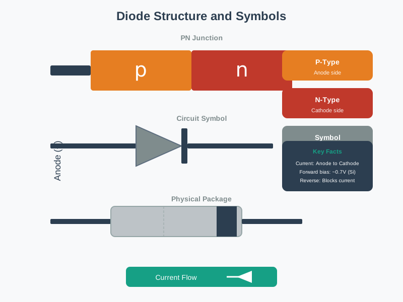
Forward
Current rises exponentially with voltage; a typical silicon diode sits near 0.6–0.7 V at everyday currents, higher when pushed hard.
Reverse
Blocks (only tiny leakage) until reverse breakdown — which Zener diodes use on purpose.
Schottky
Low forward drop (~0.3 V) and very fast; a majority-carrier device with negligible reverse recovery.
Vf drifts
At fixed current, Vf falls about 2 mV per °C as the diode warms.
That is why a "diode protected" net still needs a current path and a number. A clamp to Vcc protects the pin only if the rail can absorb or regulate the injected current; otherwise the rail can rise and back-power the device. A flyback diode protects a switch only if it is oriented to conduct after the coil is switched off. A Schottky reverse-polarity diode saves voltage drop, but its reverse leakage and lower blocking rating must still fit the product's heat, battery, and fault envelope.
Overview Knowledge Check
Practitioner: Clamp Diodes Protect an Input
Most microcontroller GPIO and ADC pins already contain two internal clamp diodes: one from the pin to Vcc and one from the pin to GND. If the pin voltage rises above about Vcc + 0.6 V, the upper diode conducts and shunts the excess into the supply rail; if it falls below about GND − 0.6 V, the lower diode conducts to ground. They keep the delicate gate inside safe limits — but they can only carry a few milliamps, so you must add a series resistor to limit the current they have to divert.
Worked example — a 5 V signal into a 3.3 V input. Feed a 5 V logic HIGH through a 10 kΩ series resistor into a 3.3 V pin. The upper clamp diode conducts once the pin exceeds about 3.3 + 0.6 = 3.9 V, holding the pin near 3.9 V. The series resistor limits the clamp current to about (5 − 3.9) / 10 kΩ = 0.11 mA — well within the clamp's rating, so the input survives.
Do the same calculation with the worst voltage, not just the friendly bench case. If the outside connector could see 12 V during a wiring mistake, the same 10 kΩ resistor gives roughly (12 − 3.9) / 10 kΩ = 0.81 mA. That may still be safe for one pin, but multiple pins clamping into an unpowered board can raise Vcc, wake devices through their protection network, or violate the rail regulator's sink-current assumption. The review item is therefore not "does it clamp?" but "where does every milliamp go?"
Relying on clamp diodes is a last-line safety net, not a design intent: sustained clamp current can back-power the rail and stress the pin. For a permanent 5 V-to-3.3 V connection, shift the level properly (a divider or a level-translator) and let the clamps only catch transients.
A Schottky diode's low ~0.3 V drop makes it the better choice for series reverse-polarity protection on a battery device, where a 0.7 V silicon drop would waste more of the pack's voltage and run hotter. For a relay, motor, or solenoid, the opposite review is needed: the flyback diode is normally reverse-biased, then becomes forward-biased when the switch opens and the coil forces current to keep flowing. Choose its forward-current, surge, and reverse-voltage ratings for that stored-energy event, and check whether slow current decay is acceptable for the actuator release time.
Practitioner Knowledge Check
Under the Hood: Temperature Drift and Reverse Recovery
Two second-order diode effects decide real designs. First, at fixed current a diode's forward voltage falls about 2 mV for every °C of warming. That is why a forward-biased diode (or a transistor's base-emitter junction) makes a cheap temperature sensor — and also why a "0.7 V drop" you budgeted at room temperature is not the same drop at 70 °C, and why simple diode voltage references drift.
That drift is useful only when it is intentional and calibrated. In a protection circuit it can move a threshold by hundreds of millivolts across an outdoor enclosure's operating range. In parallel diode paths it can also create current sharing problems: the hotter diode has a lower Vf, so it tends to steal more current, heat further, and push the pair away from equal sharing unless ballast resistance, package matching, or a different topology controls the loop.
Second, a normal silicon PN rectifier does not stop conducting instantly when it is suddenly reverse-biased: stored minority-carrier charge must be swept out first, so a burst of reverse current flows during the reverse-recovery time. Datasheets describe this with terms such as trr and recovered charge Qrr. At low frequencies that is harmless, but in a high-frequency switching converter or a fast flyback path the reverse-current pulse overlaps switch voltage and becomes real switching loss, electromagnetic noise, and heat. A general-purpose 1N400x diode can be fine on a rectified mains or slow relay path and still be the wrong part in a 100 kHz converter.
A Schottky diode conducts by majority carriers and stores essentially no such charge, so it has negligible reverse recovery — which is exactly why fast switching rectifiers use Schottky or fast-recovery parts rather than a general-purpose rectifier. The trade is not free: Schottkies usually have higher reverse leakage and lower reverse-voltage ratings than comparable PN parts. A reviewed design chooses the diode family from the waveform, temperature, leakage budget, and blocking voltage together, then checks the actual part curves instead of assuming every diode with the same current rating behaves the same.
Under-the-Hood Knowledge Check
15.4 Release Checklist
Before signing off a diode protection or switching path, verify that:
- Forward voltage is checked at the expected current and temperature, not copied as a universal
0.7 Vvalue. - GPIO or ADC clamp current is limited by a series resistor and compared with the pin’s absolute-maximum ratings.
- Sustained level shifting is handled by a divider, buffer, or translator rather than relying on internal clamps.
- Series reverse-polarity protection budgets voltage loss and heat for silicon versus Schottky choices.
- Flyback and switching diodes meet reverse-voltage, forward-current, surge, and recovery-time needs.
- Reverse-recovery loss is reviewed for PWM, switching converters, and fast inductive loads.
- Temperature drift is included when a diode drop is used as a threshold, reference, or measurement signal.
15.5 See Also
- Semiconductors, Doping, and Diodes: Return to the main chapter on junctions, devices, and transistor-switching context.
- Transistor Selection Guide: Connect diode protection choices to BJT and MOSFET switching circuits.
- Electricity Applications: Review circuit-level power, heating, and load behavior.
- Testing Environmental Conditions: Relate forward-voltage drift to temperature testing.
- Motor Control Circuits: Apply flyback and recovery choices to inductive actuator loads.
15.6 Next
After diode protection behavior is explicit, continue with Transistor Selection Guide to choose the switching device and gate/base drive around that protection path.