11 Logic Level and Level Shifting Contracts
11.1 Start Simple
Imagine a 3.3 V microcontroller connected to a 5 V sensor board. A wire that looks like a signal can still violate input thresholds, noise margin, or absolute-maximum ratings. Start by writing the HIGH and LOW voltages for both sides, then choose whether the connection can be direct, divided, buffered, or level shifted.
11.2 Learning Objectives
After this page, you should be able to:
- Compare driver output guarantees with receiver input thresholds for a digital interface.
- Calculate HIGH noise margin from VOH and VIH and explain why margin matters.
- Decide when 3.3 V to 5 V or 5 V to 3.3 V links need level shifting.
- Choose between resistor dividers, active translators, open-drain pull-ups, and MOSFET bus shifters.
- Check absolute-maximum voltage, clamp-current, rise-time, and back-powering risks before connecting boards.
11.3 Why Electronics Tools Come First
Electronics Concepts and Calculators introduces GPIO limits, signal-versus-power separation, current limiting, switching components, and protection habits. This page turns those habits into an interface contract: a digital link must meet threshold math and must not exceed any pin’s survivability limits.
Use it when a 3.3 V microcontroller talks to a 5 V sensor, a divider is proposed on a fast signal, an I2C bus crosses voltage domains, a powered module can drive an unpowered board, or a datasheet threshold must replace a guess about compatible logic levels.

Phoebe’s Why
An N-channel MOSFET is a voltage-controlled switch: the channel opens once the gate sits far enough above the source. Wire the gate to the higher rail only – the way the BSS138 bidirectional shifter this chapter describes ties its gate to the 5 V side – and the switch stops being symmetric. Pull the 3.3 V source node toward ground and the gate-to-source voltage swings wide open, so the channel does the pulling on that side immediately. Pull the 5 V drain node toward ground instead, and the gate voltage never moved; it is still anchored to 5 V through the same pull-up it is fighting, so the channel cannot yet see that pull from the drain side. What responds first is the diode built into every MOSFET’s silicon between source and drain: once the drain falls far enough below the source, that junction forward-biases and drags the source down with it. Only after the source has dropped does the gate-to-source voltage finally open the channel, which then finishes the job the diode started. Two directions, two different physical mechanisms – exactly the asymmetry this chapter’s own text describes (“the body diode first nudges the low side down, then the MOSFET turns on”) without yet showing the numbers behind it.
The Derivation
The channel opens once the gate clears the source by threshold:
\[V_{GS} = V_{CCB} - V_{S} > V_{GS(th)}\]
Low side pulled to ground drives this hard, since the gate stays fixed at \(V_{CCB}\):
\[V_{GS} = V_{CCB} - 0 = V_{CCB}\]
The body diode is a silicon PN junction from source to drain; it conducts once forward-biased past its turn-on voltage:
\[V_{S} - V_{D} > V_f, \qquad V_f \approx 0.6\text{-}0.7\ \text{V (silicon)}\]
Once the channel is open, the pulled-up node settles as a divider between the small channel resistance and the pull-up resistor:
\[V_{offset} \approx R_{DS(on)}\,\frac{V_{CCB}}{R_{pullup}}, \qquad R_{DS(on)} \ll R_{pullup}\]
Worked Numbers: This Chapter’s Own 3.3 V / 5 V, 4.7 kΩ Bus
- Low side pulls low: \(V_{GS} = 5.00 - 0 = 5.00\) V, far past a small-signal switching MOSFET’s gate threshold (typically roughly 1-3 V for parts in this class) – the channel is driven hard on.
- Resulting high-side offset: with this chapter’s own \(R_{pullup} = 4.70\ \text{k}\Omega\) and a catalog-typical switching-MOSFET channel resistance in the single-to-tens-of-ohms range at this gate drive, \(V_{offset} \approx R_{DS(on)} \times 5.00 / 4700\). Even a generous \(50\ \Omega\) gives \(V_{offset} = 50\times5.00/4700 = 0.0532\) V \(= 53.2\) mV – about 5.37% of a 0.990 V CMOS \(V_{IL}\) (\(0.3\times3.30\) V), so the exact channel resistance barely matters to the logic decision.
- High side pulls low – diode hand-off: the source sits at \(3.30\) V (this chapter’s own low rail), so the body diode turns on once the drain falls below \(3.30 - 0.65 = 2.65\) V. Below that point the diode, not the gate, is doing the work, until the falling source voltage itself opens the channel.
- Cross-check against this chapter’s own sink current: the same \(4.7\ \text{k}\Omega\) pull-up this chapter already sizes gives \(3.30/4700 = 0.702\) mA of low-side sink current, matching the chapter’s own \(0.70\) mA figure.
The two hand-offs are why a single N-MOSFET, gate tied to just one rail, can shift a bus in both directions: the channel handles the direction its gate is wired for directly, and the body diode covers the other direction just long enough to hand the job to the channel.
Overview: Four Numbers Define a Logic Interface
Two chips talk digitally only if they agree on what voltages mean 0 and 1. Every logic interface is governed by four numbers: what a driver outputs and what a receiver requires.
VOH / VOL
The driver's guaranteed output: at least VOH for a HIGH, at most VOL for a LOW.
VIH / VIL
The receiver's requirement: it reads HIGH only above VIH, LOW only below VIL.
Noise margin
The slack: NM(high) = VOH − VIH. Bigger margin rejects more noise before a bit flips.
Mismatch → shift
Different supplies (3.3 V vs 5 V) often break VOH ≥ VIH or exceed a pin's maximum — you must level shift.
A valid HIGH link needs the driver's VOH to clear the receiver's VIH; whatever is left over is the noise margin that keeps interference from being misread — the same margin that gives digital signals their noise immunity.
Worked example: an ESP32 output is powered from 3.3 V and its HIGH output is close to 3.3 V when lightly loaded. A 5 V TTL input may require only VIH = 2.0 V. The HIGH noise margin is therefore about 3.3 - 2.0 = 1.3 V. A cable transient or ground offset would have to steal more than 1.3 V before the receiver stops seeing a HIGH, so this direction is usually safe from a logic-threshold point of view.
The opposite direction is a different risk. A 5 V output connected directly to a 3.3 V microcontroller input may be read as HIGH, but it can exceed the input's absolute maximum rating. A correct review separates "will the bit be interpreted correctly?" from "will the pin survive?" That is why a circuit note should list both threshold margin and absolute-maximum protection, not just a casual statement that the voltages are close enough.
For beginner IoT boards, the practical checklist is simple: identify the driver supply, receiver supply, guaranteed output levels, required input thresholds, and pin maximum voltage. If any number is missing, do not assume compatibility. Look up the datasheet, add a level shifter, or constrain the interface to an open-drain bus with the correct pull-up rails.
Overview Knowledge Check
Practitioner: Shifting Down Is Easy, Shifting Up Is Not
The two directions are not symmetric. Going down (5 V → 3.3 V) mainly protects the lower-voltage input, whose absolute maximum is only a little above its own supply. For a slow, unidirectional push-pull signal a resistor divider is enough:
Vout = Vin × R2 / (R1 + R2). Put R1 = 1 kΩ in series from the 5 V signal and R2 = 2 kΩ to ground: Vout = 5 × 2 / (1 + 2) = 3.33 V — a safe HIGH for the 3.3 V input.
Going up (3.3 V → 5 V) is different. If the 5 V receiver is CMOS it needs VIH ≈ 0.7 × 5 = 3.5 V, and a 3.3 V output falls just short. A resistor divider cannot help — dividers only attenuate, never add voltage. You need something active: a MOSFET or transistor level-shifter, a dedicated level-translator IC, or an open-drain line with its pull-up tied to 5 V so the HIGH is pulled up to the higher rail.
Do not choose divider values by ratio alone. The divider above has total resistance 3 kΩ, so it draws 5 V / 3 kΩ = 1.67 mA whenever the input is HIGH. That is acceptable on a bench, but wasteful for a sleeping battery node. Scaling to 10 kΩ and 20 kΩ keeps the same 3.33 V output while reducing divider current to 0.167 mA. The tradeoff is edge speed: with 20 pF of input plus wiring capacitance, the Thevenin resistance is about 6.7 kΩ, giving an RC time constant near 134 ns. That is fine for a slow enable pin, but not a reason to use dividers casually on fast buses.
A practitioner review should also name the signal direction. A unidirectional "5 V interrupt output into ESP32 GPIO" can use a divider or translator. A bidirectional "3.3 V MCU and 5 V sensor share I2C" cannot be reviewed as two independent one-way signals, because either side may pull the line low. In that case, choose a bidirectional MOSFET shifter or a translator IC and size pull-ups for the bus speed and capacitance.
| Direction | Concern | Typical solution |
|---|---|---|
| 5 V → 3.3 V (down) | Overvoltage on the 3.3 V input | Resistor divider (slow, one-way) or a level-translator |
| 3.3 V → 5 V (up) | 3.3 V may be below the 5 V part's VIH | Active shifter, translator IC, or open-drain pulled up to 5 V |
Practitioner Knowledge Check
Under the Hood: Bidirectional Buses and Absolute Maximums
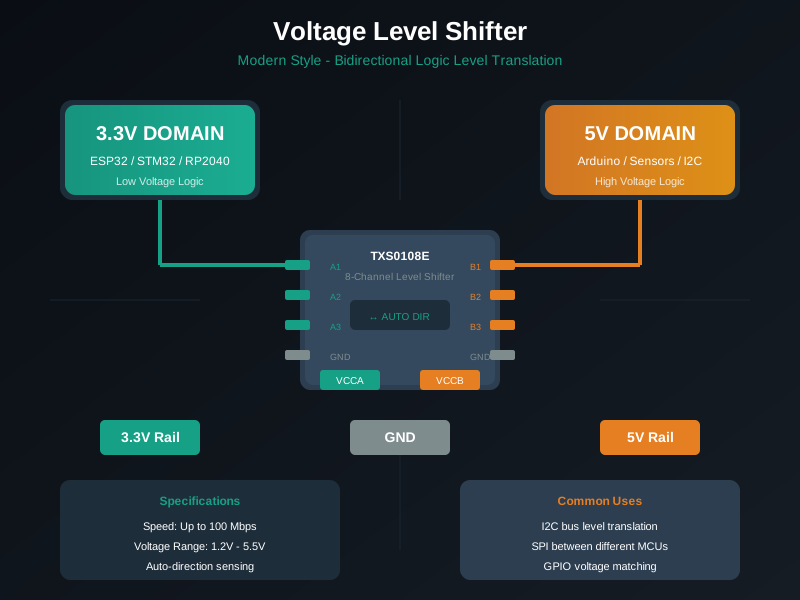
A resistor divider is not just up-shift-incapable — it is also unidirectional and speed-limited (its resistance and the line capacitance form an RC that softens fast edges). That fails a shared bus like I2C, where both sides must be able to drive the line. The standard trick is to make the lines open-drain with a pull-up on each side and place a single N-channel MOSFET per line (the classic BSS138 bidirectional shifter): when either side pulls low, the MOSFET couples the low across, and when released each side floats up to its own rail. That is why bus level-shifting looks different from a simple signal divider.
The reason down-shifting is mandatory, not optional, is the absolute-maximum input rating: a 3.3 V pin usually tolerates only about Vcc + 0.3 to 0.5 V before its internal clamp diodes conduct hard and it risks damage or back-powering its own rail. So drive a lower-voltage input from a higher-voltage source only through a proper shift — never by trusting the clamp diodes to survive a continuous overvoltage.
The MOSFET bus shifter works because the body diode and gate bias make a low level propagate across domains while released lines rise independently. On a 3.3 V / 5 V I2C link, the low side is pulled up to 3.3 V and the high side to 5 V. If the 3.3 V device pulls SDA low, the MOSFET conducts and drags the 5 V side low too. If the 5 V device pulls low, the body diode first nudges the low side down, then the MOSFET turns on and completes the low-level transfer. When neither device pulls, each side returns to its own safe HIGH.
Pull-up sizing is part of the evidence. With 4.7 kΩ pull-ups to 3.3 V, each LOW sinks about 3.3 V / 4.7 kΩ = 0.70 mA on that side. Stronger pull-ups such as 2.2 kΩ sharpen edges but increase sink current; weaker pull-ups reduce current but may fail rise-time limits on long wires. If a sensor board works at 100 kHz on a short jumper but fails at 400 kHz after the harness is installed, the level shifter may be electrically correct while the RC rise time is still too slow.
A final under-the-hood trap is back-powering. If a powered 5 V module drives a line into an unpowered 3.3 V microcontroller through its protection diode, the microcontroller rail can rise partially even though its regulator is off. That can create ghost boot states and latch-up risk. A robust design avoids continuous clamp current, sequences rails deliberately, or uses a translator with power-off isolation.