23 ADC Architecture and Resolution
23.1 Start Simple
Imagine two ADCs with the same number of bits but different internal behavior. A SAR ADC may need a low-impedance source that settles quickly, while a sigma-delta ADC trades speed for noise performance through oversampling. Start with the signal bandwidth, source impedance, noise target, and conversion time before choosing an architecture.
23.2 Learning Objectives
After this page, you should be able to:
- Choose SAR or sigma-delta ADCs based on speed, resolution, latency, and IoT signal bandwidth.
- Calculate least significant bit size and separate converter resolution from usable measurement accuracy.
- Check SAR source impedance, sample-capacitor settling, and acquisition-time constraints before trusting readings.
- Use oversampling only when throughput and dither/noise conditions can support extra effective bits.
- Explain how sigma-delta noise shaping and decimation turn fast low-resolution samples into slow high-resolution readings.
23.3 Why This Follows How ADCs Work
How ADCs Work builds the main conversion model: sample an analog voltage, quantize it against a reference, encode a digital code, and match converter resolution to sensor needs. This page tightens that model into design contracts for real hardware.
Use it when a product decision depends on SAR versus sigma-delta architecture, a resistor divider or weak sensor may not drive the ADC input quickly enough, or a data sheet promises more bits than the sensor, reference, and sample budget can actually deliver.

Phoebe’s Why
Further down this page, plain oversampling buys about 3 dB per doubling of the oversampling ratio, a first-order sigma-delta loop buys about 9 dB, and a second-order loop buys about 15 dB – but a modulator does not work in decibels. It pushes the quantization noise’s spectral energy toward high frequency, away from the signal band, using the same feedback idea as the sigma-delta loop this page already describes. The in-band leftover – the part the decimation filter cannot remove – is what those numbers describe, and it shrinks faster and faster as the loop order rises.
The Derivation
An \(L\)-th order noise-shaping loop has noise transfer function \(\mathrm{NTF}(z) = (1-z^{-1})^L\), with magnitude-squared
\[|\mathrm{NTF}(e^{j\omega})|^2 = \left(2\sin\frac{\omega}{2}\right)^{2L}\]
Quantization noise is flat with total power \(q^2/12\) across the Nyquist band. Deep inside the oversampled signal band, \(\omega\) is small, so \(\sin(\omega/2)\approx\omega/2\) and \(|\mathrm{NTF}|^2\approx\omega^{2L}\). Integrating that rising power law over the narrow in-band window (width \(\propto 1/\mathrm{OSR}\)) gives in-band noise power \(\propto 1/\mathrm{OSR}^{2L+1}\). Doubling OSR then divides in-band noise power by \(2^{2L+1}\), an SNR gain of
\[\Delta\mathrm{SNR}_{dB} = 10\log_{10}\!\left(2^{2L+1}\right) = (2L+1)\times 3.01\]
Worked Numbers: This Page’s Own OSR 64 and 128 Cases
- \(L=0\) (plain oversampling): \((2\cdot 0+1)\times 3.01 = 3.01\) dB/octave – matches this page’s “+3 dB per octave,” \(0.5\) bit each doubling.
- \(L=1\) (first-order shaping): \(3\times 3.01 = 9.03\) dB/octave – matches this page’s “+9 dB per octave,” \(1.50\) bits each doubling.
- \(L=2\) (second-order shaping): \(5\times 3.01 = 15.05\) dB/octave – matches this page’s “+15 dB per octave,” \(2.50\) bits each doubling.
- This page’s own worked example, \(\mathrm{OSR}=64=2^6\), first-order: \(6\times 9.03 = 54.2\) dB \(\Rightarrow 54.2/6.02 = 9.00\) extra bits, exactly the “close to 9” this page states.
- Doubling to \(\mathrm{OSR}=128\) adds one more octave: \(+9.03\) dB \(= +1.50\) bits, matching this page’s own “\(1.5\)” figure exactly.
Overview: Two Ways to Spend Silicon — Speed vs Resolution
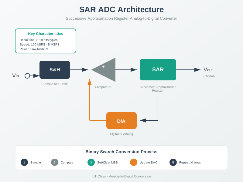
SAR and sigma-delta (ΣΔ) converters do the same job — turn a voltage into a code — but spend the silicon on opposite ends of the same trade. A SAR ADC runs a binary search: for an N-bit result it makes N comparisons against an internal DAC, one bit per clock, so one sample takes about N clocks and the answer is ready the moment the last bit is decided. A ΣΔ ADC instead runs a coarse (often 1-bit) quantizer very fast, then uses a digital filter to average that stream down into many effective bits.
Both share the same finest step: the least significant bit is LSB = Vref / 2^N. What differs is how each reaches that step and what it costs. A 12-bit SAR on an ESP32, STM32, or AVR converts in microseconds with no filter delay; a 24-bit ΣΔ like the HX711 (load cells) needs milliseconds because it trades sample rate for resolution.
Worked example. Suppose a 0–3.3 V pressure sensor outputs 1.65 V at half scale. A 12-bit SAR code is approximately round(1.65 / 3.3 * 4095) = 2048. One code is 3.3 / 4096 = 0.806 mV, so random jitter of three codes is only about 3 * 0.806 = 2.42 mV. That is fine for a pressure switch or a battery monitor. A load cell bridge is different: its full-scale signal may be only a few millivolts, so a 2.42 mV wobble can hide the measurement. That is where the slow ΣΔ path earns its keep.
SAR ADC
Binary search, N comparisons per sample. Fast (kSPS–MSPS), medium resolution (8–16 bit), low latency. Built into most microcontrollers.
Sigma-Delta
Oversample a 1-bit quantizer, then noise-shape and decimate. Slow (SPS–kSPS), very high resolution (16–24 bit), filter latency.
Resolution (LSB)
LSB = Vref / 2^N. For a 12-bit ADC at Vref = 3.3 V, the LSB is 3.3 / 4096 = 0.806 mV. Resolution is not accuracy.
Which When
Fast-changing signals (audio, vibration, motor) → SAR. Slow precision DC (strain, thermocouple, load cell) → ΣΔ.
Overview Knowledge Check
Practitioner: The Two Constraints That Bite in Real Circuits
Each architecture has one constraint that quietly ruins readings if ignored: the SAR needs its input to settle in time, and the ΣΔ (or any oversampling scheme) needs the right amount of noise and time to buy resolution.
| Architecture | Hidden constraint | Practical rule |
|---|---|---|
| SAR | The sample-and-hold capacitor must charge through the source resistance before the first bit decision. | Keep source resistance low (single-digit kΩ or less) or add an op-amp buffer; otherwise lengthen the acquisition time. |
| Sigma-delta / oversampling | Extra bits cost samples and need dither noise to exist at all. | To gain w bits, sum 4^w samples and shift right by w; throughput drops by 4^w. |
SAR settling. The internal sample cap charges with time constant τ = R_source × C_sample. To settle within half an LSB of an N-bit result the input needs about (N+1) × ln 2 time constants — roughly 9 time constants for a 12-bit conversion. If the sensor node is high-impedance (a resistor divider or a weak sensor output), τ is large, the cap never finishes charging in the acquisition window, and every reading reads low. This is why a high-impedance source needs a buffer ahead of the ADC, and it is the mechanism behind the "input impedance mismatch" pitfall.
Worked example — turning a 12-bit SAR into ~14 bits by oversampling. Averaging trades speed for resolution: to add w bits, take 4^w samples, sum them, and shift the sum right by w. For w = 2 that is 4^2 = 16 samples summed (max 16 × 4095 = 65520, a 16-bit sum) and shifted right by 2, giving a ~14-bit value — at 1/16 of the original sample throughput.
This only works if the signal carries at least about 1 LSB of noise. That noise acts as dither: it spreads a between-codes voltage across neighbouring codes, so the average lands between them. A perfectly clean, noise-free DC input sits on one code forever and averaging buys nothing.
Practitioner Knowledge Check
Under the Hood: Why a 1-Bit Converter Can Reach 24 Bits
A sigma-delta modulator feeds a coarse quantizer (often just 1 bit) from an integrator that is driven by the difference between the input and the fed-back quantizer output. That feedback loop has a crucial side effect: it shapes the quantization noise, pushing most of it up to high frequencies, out of the band where the signal lives. A digital low-pass decimation filter then throws that high-frequency noise away and drops the sample rate, leaving a high-resolution, low-rate output.
The numbers make the trade concrete. An ideal N-bit quantizer driven by a full-scale sine has SNR = 6.02 N + 1.76 dB (so each extra bit is worth about 6 dB). Oversampling spreads a fixed amount of quantization noise over a wider band, so the in-band noise falls:
- Plain oversampling, no shaping: about
+3 dB per octaveof oversampling ratio — that is only+0.5 biteach time you double the sample rate (equivalently+1 bit per 4×). - First-order noise shaping: about
+9 dB per octave— roughly+1.5 bitsper doubling of the oversampling ratio. - Second-order noise shaping: about
+15 dB per octave— roughly+2.5 bitsper doubling.
Worked example. A first-order ΣΔ modulator sampled with oversampling ratio 64 has six doublings above base rate (2^6). At about 9 dB per doubling, the shaped-noise benefit is roughly 6 * 9 = 54 dB. Since one ideal bit is about 6.02 dB, that is close to 54 / 6.02 = 9 extra effective bits before real-world limits such as clock jitter, reference noise, and analog front-end noise reduce the result. Doubling the ratio to 128 adds one more octave, so the ideal gain is another 9 dB, or about 1.5 bits.
This is how a modulator with a 1-bit quantizer running at a high oversampling ratio, with second- or higher-order shaping, ends up delivering 20+ effective bits. A SAR, by contrast, does not average: each conversion is complete on its own, so its ceiling is set by DAC and comparator matching and by reference-voltage quality (the DNL/INL of the part), not by how long you oversample.
Under-the-Hood Knowledge Check
Release Checklist
Before signing off an ADC architecture choice, verify that:
- The selected ADC architecture matches the signal: SAR for low-latency moderate-resolution signals, sigma-delta for slow precision DC, and flash only for extreme speed.
-
LSB size is calculated from
Vref / 2^Nand compared with sensor accuracy, reference noise, and analog-front-end noise. - SAR acquisition time is long enough for the source impedance and sample capacitor to settle within the target error band.
- Any high-impedance divider or sensor output is buffered, slowed, or sampled with an acquisition time supported by the data sheet.
-
Oversampling budgets the
4^wsample-count cost for each additional effective bit and confirms that enough dither/noise exists. - Sigma-delta latency, decimation-filter delay, and update rate are acceptable for the control loop or telemetry interval.
- Effective resolution is documented as ENOB or measured noise-free counts rather than copied from headline bit depth.
See Also
- How ADCs Work: Return to the main ADC fundamentals chapter for conversion flow, formulas, and selection context.
- Nyquist Sampling Theory: Connect converter choice to sample-rate and anti-aliasing requirements.
- ADC/DAC Worked Examples: Practice converter, reference, and resolution calculations in complete designs.
- Sensor Calibration Lab: Measure offset, gain, and noise once hardware is built.
- Sensor Fundamentals: Match sensor output range and impedance to the ADC front end.
Next
After the ADC architecture contract is explicit, continue with Nyquist Sampling Theory to choose sample rates and anti-aliasing filters for time-varying signals.