9 Serial Bus Interface Contracts
9.1 Start Simple
Imagine adding one sensor module to a microcontroller and needing the reading to arrive every time. The bus choice is a promise about wires, voltage levels, addresses or chip selects, timing, and recovery when the device misbehaves. Start with distance, speed, device count, and the failure mode you can debug in the field.
9.2 Learning Objectives
After this page, you should be able to:
- Select I2C, SPI, or UART from pin count, speed, addressing, and wiring constraints.
- Explain why I2C uses open-drain outputs and pull-up resistors on shared wires.
- Calculate UART byte timing from baud rate and frame format.
- Diagnose I2C rise-time limits from bus capacitance, pull-up strength, and sink-current limits.
- Explain how SPI chip-selects and CPOL/CPHA modes affect multi-device links.
9.3 From Electricity to Electronics
From Electricity to Electronics maps the electronics building blocks behind IoT hardware: semiconductors, diodes, transistors, GPIO limits, drivers, and protection components. This page turns those blocks into the bus-level contract that connects sensors and peripherals to the microcontroller.
Use it when a board must choose between I2C, SPI, and UART, a sensor bus fails after adding cable length or more devices, SPI returns garbage because of mode mismatch, or a UART link drops frames because the baud and framing assumptions are not identical.

Phoebe’s Why
I2C’s open-drain HIGH is not driven; it is released and left to a passive pull-up charging the bus capacitance, exactly as this chapter says. That charging is a first-order RC transient – the same exponential this chapter’s own strong/weak pull-up tradeoff runs on – and an RC transient does not know or care what the clock frequency is. The clock is the thing that decides how much of that transient’s time budget actually exists. This chapter names both of I2C’s own speeds, Standard 100 kHz and Fast 400 kHz, and a clock period is nothing but the reciprocal of frequency: quadruple the frequency and the whole period, along with any fixed share of it set aside for the rising edge, shrinks to a quarter. Whatever pull-up value comfortably charged the bus in time at 100 kHz has to shrink by roughly that same factor to keep pace at 400 kHz on the same bus capacitance – which is exactly this chapter’s own claim that raising the clock forces either a stronger pull-up or a smaller bus, stated now as arithmetic instead of a rule of thumb.
The Derivation
Clock period from frequency:
\[T = \frac{1}{f}\]
Open-drain rise through a pull-up into bus capacitance, sampled between the 0.3-0.7 \(V_{DD}\) thresholds I2C actually uses:
\[V(t) = V_{DD}\left(1-e^{-t/RC}\right), \qquad t_r \approx 0.847\,RC\]
If a fixed share \(k\) of the period is budgeted for that rise, \(t_r = kT = k/f\), solving for the pull-up:
\[R = \frac{k}{0.847\,f\,C}\]
Holding \(k\) and \(C\) fixed, \(R\) scales as \(1/f\) – exactly the inverse relationship this chapter states in words.
Worked Numbers: This Chapter’s Own 100 kHz / 400 kHz Speeds
- Periods from this chapter’s own two named speeds: \(T = 1/f\) gives \(1/100{,}000 = 10.0\ \mu\text{s}\) at Standard mode and \(1/400{,}000 = 2.50\ \mu\text{s}\) at Fast mode – a \(10.0/2.50 = 4.00\times\) ratio, matching the \(400/100 = 4.00\times\) frequency jump exactly.
- Illustrative rise-time budget (an illustrative \(k=10\%\) of the period reserved for the edge, not a fixed standard): \(1000\) ns available at \(100\) kHz versus \(250\) ns at \(400\) kHz – the same \(4.00\times\) shrink.
- Required pull-up for an illustrative \(C=100\) pF bus (a modest multi-sensor stub, catalog-typical order of magnitude): \(R = 1000\text{ns}/(0.847\times100\text{pF}) = 11{,}800\ \Omega \approx 11.8\ \text{k}\Omega\) at \(100\) kHz, falling to \(R = 250\text{ns}/(0.847\times100\text{pF}) = 2950\ \Omega \approx 2.95\ \text{k}\Omega\) at \(400\) kHz – again a \(4.00\times\) drop, on the identical bus.
- Contrast with UART: this chapter’s own \(9600\) baud, 8N1 byte time (\(10\times1/9600 = 1.04\) ms) is a pure clockless timing budget with no RC term at all, because UART’s push-pull driver actively forces both edges instead of waiting on a passive charge – the reason its failure mode is baud mismatch, not bus capacitance.
The lesson is not “use \(11.8\ \text{k}\Omega\)” – the real bus capacitance sets the real number. The lesson is that every doubling of I2C clock speed halves the pull-up value a given bus capacitance can tolerate, which is precisely why this chapter tells you to count capacitance and choose the clock together, not as two independent decisions.
Overview: How the Electronics Reach the Microcontroller
The building blocks in this module — open-drain outputs, pull-ups, push-pull drivers, logic levels — come together in the three serial buses that connect almost every IoT sensor and peripheral to its microcontroller. Each bus's electrical style follows directly from those blocks.
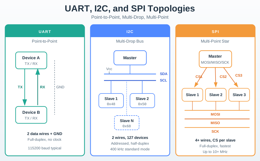
Think of the bus as a contract between the board schematic, the firmware driver, and every device on the connector. The schematic promises which pins exist, whether a line is shared, where pull-up resistors live, and how much capacitance the trace and cable add. The firmware promises the bus speed, address, chip-select timing, SPI mode, UART frame, retry behavior, and timeout policy. The peripheral promises the electrical levels it can tolerate and the protocol timing it will obey. A design is reliable only when all three promises match; a sensor can be listed as "I2C compatible" and still fail if the board used weak pull-ups across a long harness or if the driver never handles clock stretching.
The practical decision is therefore not "which bus is modern?" but "which failure mode can this product afford?" I2C saves pins and keeps multi-sensor boards tidy, but shared open-drain wires make every device and every centimeter of copper part of the same RC edge. SPI gives deterministic high-speed transfers to displays, radios, flash, or ADCs, but each added peripheral consumes routing and chip-select discipline. UART is simple and debuggable with a USB adapter or logic analyzer, yet it is best treated as point-to-point unless another layer adds addressing, framing, and collision control. Pick the bus whose electrical contract matches the product's distance, speed, device count, and service access.
I2C
Two shared wires (SDA, SCL), open-drain with pull-ups, devices selected by a 7-bit address.
SPI
Four wires (SCLK, MOSI, MISO, CS), push-pull, full-duplex, fast, one chip-select per device.
UART
Two wires, no shared clock; both ends agree a baud rate and a frame format.
The trade
Pins vs speed vs number of devices — each bus optimizes a different corner.
Overview Knowledge Check
Practitioner: The Numbers That Define Each Bus
| Bus | Wires | Selection | Key parameters |
|---|---|---|---|
| I2C | 2 (SDA, SCL), shared | 7-bit address (2^7 = 128, ~112 usable after reserved) |
Standard 100 kHz / Fast 400 kHz; a slow device holds SCL low to clock-stretch |
| SPI | 4 (SCLK, MOSI, MISO, CS) | One chip-select line per device | Full-duplex, tens of MHz; master and slave must match one of 4 modes (CPOL/CPHA) |
| UART | 2 (TX, RX), point-to-point | None (one-to-one link) | Agreed baud rate and frame, e.g., 9600 8N1 |
Worked example — UART framing at 9600 8N1. "8N1" means 8 data bits, no parity, 1 stop bit, wrapped by 1 start bit — 10 bit-times per byte. At 9600 baud each bit lasts 1 / 9600 = 104 µs, so one byte takes about 10 × 104 µs = 1.04 ms, giving roughly 960 bytes/s. Because there is no clock wire, both ends must be set to the same baud and frame or the receiver samples the bits at the wrong instants.
I2C's 2^7 address space is why you can hang a dozen sensors on two wires, while SPI trades that for speed by giving every device its own chip-select line.
Use a quick sizing pass before committing the schematic. For I2C, count every device input pin, connector stub, cable, and ESD part as bus capacitance; then choose pull-ups that meet rise-time at the selected clock while keeping LOW-level sink current inside the weakest device rating. If two sensors have the same fixed address, the design needs a different variant, a bus switch, a second controller bus, or SPI/UART instead of hoping firmware can separate them. For SPI, count one chip-select per peripheral plus any reset or data-ready lines, then verify the controller and peripheral sample on the same CPOL/CPHA edge before board bring-up. For UART, write the exact frame in the interface record: baud, data bits, parity, stop bits, voltage level, connector pinout, and whether the link is idle-high TTL, RS-232, RS-485, or another physical layer.
Bring-up evidence should match the contract. An I2C scan proves addresses acknowledge, but it does not prove the rise time is legal under worst-case temperature and cable length. A successful SPI register read proves chip-select and mode for one command, but it does not prove long bursts, shared MISO tri-state behavior, or maximum clock rate. A UART terminal prompt proves baud alignment, but it does not prove binary framing, flow control, or recovery after a reset. Capture one short logic-analyzer trace for the selected bus early; it turns abstract settings into visible edges, addresses, chip-select windows, and start/stop bits that other engineers can review.
Practitioner Knowledge Check
Under the Hood: Each Bus's Electrical Catch
The buses inherit both the strengths and the limits of their output style. I2C is open-drain, so every rising edge is driven only by the passive pull-up charging the bus capacitance (an RC curve). Add many devices or long traces and the total capacitance grows, the rising edge slows, and you must lower the clock or use a stronger pull-up (within each device's sink limit) to keep 400 kHz reliable. Clock stretching — a slave holding SCL low — lets a busy device pause the master rather than lose data.
SPI is push-pull, so it drives both edges hard and reaches far higher clock rates, but it pays in pins (a chip-select per device) and demands that master and slave agree on the clock polarity and phase (CPOL/CPHA); pick the wrong mode and every bit is sampled on the wrong edge, returning garbage. UART has no clock line at all, so its Achilles heel is the baud rate: if the two ends differ by more than a few percent, the accumulated timing error walks the sampling point off the bits and the frame decodes as noise.
The deeper reason these failures look different is that the receiver decides truth at a specific voltage and instant. On I2C, a controller samples SDA while SCL is HIGH, so a slow SDA rise can be read as LOW even though the firmware "released" the line. Lower-value pull-ups sharpen that edge, but the trade is higher sink current whenever any device pulls LOW; the smallest peripheral on the bus sets the safe limit. On SPI, edges are actively driven, so capacitance is less often the first limit on a short board, but ringing, skew, and chip-select setup/hold time matter as clocks climb. A MISO line that is not high impedance when its device is deselected can corrupt every other peripheral, even if each part works alone on the bench.
UART hides a different timing budget inside the frame. The receiver detects the falling start bit, waits toward the middle of each bit cell, and then samples data without seeing another clock edge. Any baud mismatch, oscillator drift, interrupt latency, or long cable distortion accumulates across the byte until the stop bit is sampled too early or too late. That is why a forgiving console link may work at 9600 baud but fail at 921600 baud, and why field products often use explicit packet framing, checksums, and reset recovery around UART streams. The bus choice is therefore a system reliability choice: each protocol moves the risk to a different place in the electrical and firmware stack.