Prototyping · Study deck
PCB Design and Fabrication
A PCB is not just a neat version of a breadboard.
Voltage Vera is your guide for this deck.
After studying this chapter
Learning objectives
You will be able to:
- Decide when breadboard evidence is strong enough to move into a custom PCB stage.
- Review a schematic and footprint set before layout begins.
- Place and route components using power, return-path, connector, sensor, and radio constraints.
- Prepare a fabrication and assembly package that another builder can inspect.
Major section
In 60 Seconds · Start With the Story
A PCB is not just a neat version of a breadboard.
- Moving from breadboard to PCB feels like progress, but it can also freeze every untested assumption into copper.
- A stable sensor reading on loose wires does not prove footprint orientation, reset access, antenna keep-out, regulator heat, connector strain, or first-power bring-up.
- Schematic checks, footprint review, layout constraints, fabrication outputs, and bring-up notes all exist to make the first board teach the next revision instead of hiding the cause of failure.
Major section
Phoebe's Field Notes: Why Copper Isn't Just Copper Once It's a Trace · PCB Freezes Assumptions
Skin depth is 92.3 µm at 500 kHz but only 2.16 µm at 915 MHz, so a DC trace rule cannot stand in for an RF layout rule.
- A working demo cannot substitute for tests of the new physical paths.
Major section
Check Manufacturing Package
For a prototype board, KiCad, Altium Designer, Eagle, EasyEDA, or another EDA tool is only the source.
- The handoff includes generated outputs that must agree with the revision being built.
- A correct schematic symbol is not enough if the ordered switch, sensor, regulator, or JST connector is a different footprint variant.
- That note is what turns a failed first board into useful design evidence.
Major section
Layout Quality Needs Current Loops
The PCB decides how current returns, how noise couples, how heat leaves, and whether a human can debug the board.
- RF and sensors: respect antenna keep-outs, ground clearance, sensor exposure, thermal isolation, ESD paths, and enclosure materials that change readings.
- The first board is successful when it teaches the next revision quickly, not merely when it arrives from the fabricator.
- The loop view explains why two layouts with the same schematic can behave differently.
Major section
Layout Quality Needs Current Loops (continued)
A board can pass DRC while still burying the antenna under a battery, enclosure post, cable, or ground pour.
- A buck regulator's high-current switching loop should be short, with the input capacitor, switch, diode or synchronous path, inductor, and ground return placed so current does not travel across the sensor area.
- Layout review is therefore part electrical review and part physical evidence review.
- Service access is also a circuit decision.
Major section
Layout Planning
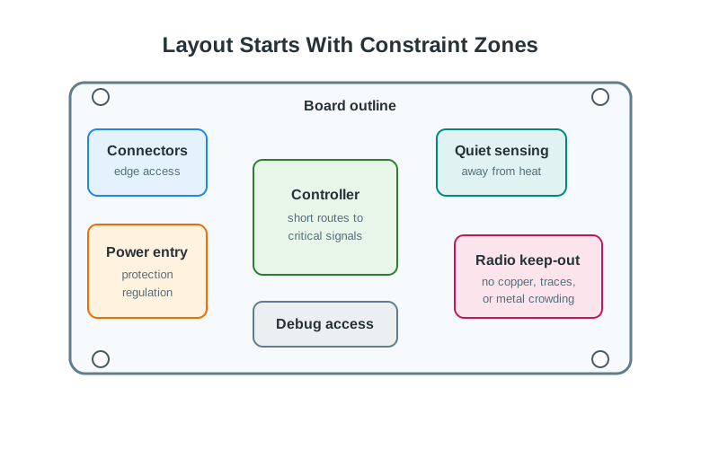
Good layout starts with zones.
- Connectors, power entry, radio or antenna areas, sensors, high-current loads, quiet analog circuits, and debug access should not compete for the same space.
- Connectors belong where the enclosure and harness can reach them.
- The power entry, protection, and regulators need a short path that can be inspected before signals cross the board.
Major section
Layout Planning (continued)
The controller and quiet analog sensing area should be placed with noise and routing in mind; the radio antenna needs its keep-out region.
- Debug access must remain reachable after assembly.
- A placement that hides a rail test point or violates the antenna area can make first-article evidence weak even when design rules pass.
- Debug stays reachable: Programming, reset, boot selection, serial logs, and measurement points should remain usable after partial assembly.
Major section
Power, Ground, and Return Paths
Most first-board failures are not caused by the schematic being completely wrong.
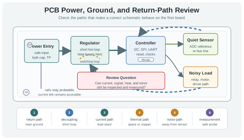
- The nearby ground return keeps fast current loops short, while the quiet sensor route stays apart from relay or motor noise.
- Thermal copper, airflow, and spacing provide a separate escape path for heat.
- Layer count is an engineering tradeoff, not a badge.
Major section
Power, Ground, and Return Paths (continued)
The board is ready only when each physical path can be traced and tested.
- Decoupling path: Each power pin has a short loop through its local capacitor and ground return before joining the wider rail.
- Thermal path: Regulators, drivers, protection parts, and power resistors have copper area, airflow, or spacing appropriate to their dissipation.
- Noise path: Switching loops, relay coils, motor paths, and load transients are kept away from sensor and reference nodes.
Major section
Layer Review Question · Fabrication and Assembly Package
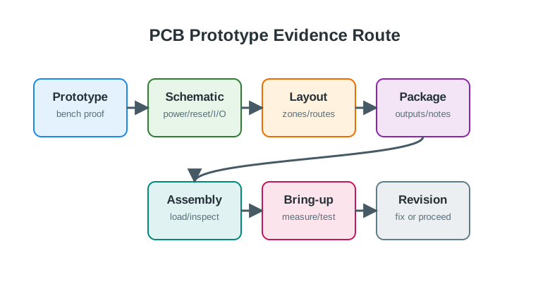
The fabrication package is the handoff from design intent to board production.
- It should be complete enough for someone else to inspect, fabricate, assemble, and bring up the board without guessing which file is authoritative.
- The manufacturing set includes copper, mask, silkscreen, paste, and drill outputs.
- the PCB Design Flow diagram shows what must travel with a reviewed board revision.
- A schematic and layout review checks footprints against physical parts, then ERC, DRC, and unconnected-net results expose design errors before fabrication.

Major section
First Article Bring-Up
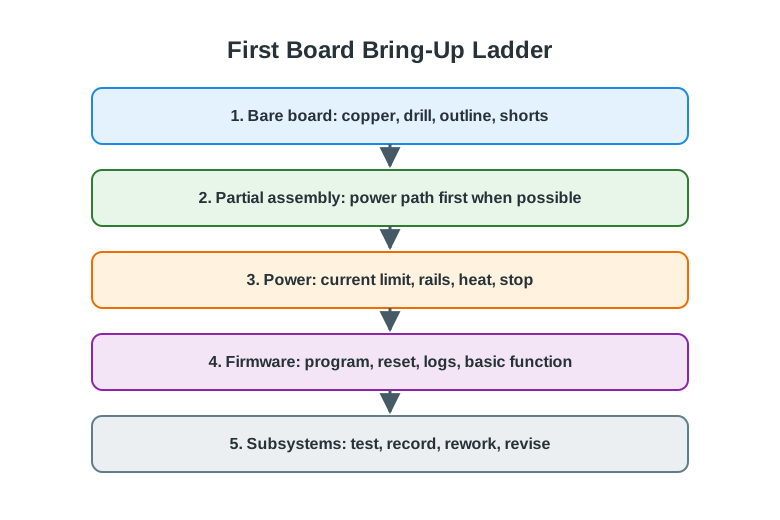
The first assembled board should be brought up in small steps.
- The goal is to localize faults before they damage parts or bury the evidence under full firmware behavior.
- Figure: A first-article soldering setup shows a hot iron shows the tools needed for controlled first-article soldering.
- Prepare the iron with a clean, tinned tip, use enough heat to wet the pad and lead quickly, and keep cleaning and re-tinning the tip as flux and oxide build up.
- the A first-article soldering setup shows a hot iron beside a spring stand, cleaning sponge and spool of solder. The photo makes the stand and tip-cleaning supplies visible on a plain bench diagram shows the tools needed for controlled first-article soldering.
Major section
First Article Bring-Up (continued)
The iron tip makes the joint, while the coiled stand keeps the hot tool off the bench between joints.
- Cleaning material and solder help keep the tip wettable; nearby hand tools let the builder place and inspect parts without improvising around heat.
- Those visible tools support assembly, but they cannot prove a new PCB works.
- For the first amplifier board, compare placement with the design record, check continuity and rails, then power with a current limit.

Major section
First Article Bring-Up (continued)
An LED or other simple indicator can show whether the output crosses the expected threshold, but it should be read as a test result, not as proof of the whole analog design.
- If the breadboard passes and the PCB fails, isolate the difference: feedback resistor values, input polarity, op-amp channel pins, supply reference, solder bridges, and whether the output load changes the amplifier behavior.
- Assemble the power path first when possible, then apply power through a current limit and check rails, heat, and the stop condition.
- This order protects the board and makes a failed first article useful for the next revision.
Major section
Incremental Examples
A breadboarded ESP32-C3 sensor node uses a known SHT31 module, a JST battery connector, a programming header, and one status LED.
- The first PCB should be a carrier board that reduces wiring risk without pretending the design is production-ready.
- The main evidence is whether the PCB removes wiring ambiguity while keeping debug access visible.
- Assemble power and programming sections first, then add the sensor and radio path only after rail current, reset behavior, and SWD access are proven.
Major section
Incremental Examples (continued)
This case is harder because footprint and layout decisions can change the measurement.
- A correct schematic is not enough if the sensor is heated by the regulator or the debug pads disappear under the enclosure.
- A team has a functional prototype that samples vibration and temperature, logs local events, and reports summaries through a nearby gateway.
- Footprint gate: Connectors, sensor package, mounting holes, switch orientation, and enclosure clearances are checked against physical parts.
Deck summary
Key takeaways
A PCB is not just a neat version of a breadboard.
- Skin depth is 92.3 µm at 500 kHz but only 2.16 µm at 915 MHz, so a DC trace rule cannot stand in for an RF layout rule.
- For a prototype board, KiCad, Altium Designer, Eagle, EasyEDA, or another EDA tool is only the source.
- The PCB decides how current returns, how noise couples, how heat leaves, and whether a human can debug the board.
- A board can pass DRC while still burying the antenna under a battery, enclosure post, cable, or ground pour.
Retrieval practice
Recall check 1 of 4
Voltage Vera says: answer from memory, then check your reasoning.
Q1A board schematic is correct, but a radio transmit burst resets the sensor controller. Which layout review matters?
Show answer
Answer: B PCB current paths can disturb a correct logical circuit.
Retrieval practice
Recall check 2 of 4
Voltage Vera says: answer from memory, then check your reasoning.
Q2A breadboard circuit is ready for PCB layout. Which review should happen before routing?
Show answer
Answer: A These checks catch errors that layout would otherwise freeze into copper.
Retrieval practice
Recall check 3 of 4
Voltage Vera says: answer from memory, then check your reasoning.
Q3A breadboard prototype works, and the team wants to create a custom PCB. What is the strongest reason to move into the PCB stage?
Show answer
Answer: C A PCB is justified when it answers evidence questions that a breadboard cannot answer reliably.
Retrieval practice
Recall check 4 of 4
Voltage Vera says: answer from memory, then check your reasoning.
Q4During first power on a new PCB, the current-limited supply immediately hits the limit and the 3.3 V rail does not rise. What should the team do next?
Show answer
Answer: B First bring-up should localize power faults before sensitive loads or full firmware hide the evidence.
Print reference
Answers
Answer key.
- B · PCB current paths can disturb a correct logical circuit.
- A · These checks catch errors that layout would otherwise freeze into copper.
- C · A PCB is justified when it answers evidence questions that a breadboard cannot answer reliably.
- B · First bring-up should localize power faults before sensitive loads or full firmware hide the evidence.