19 Analog-Digital Signal Boundary Contracts
19.1 Start Simple
Imagine a noisy sensor voltage arriving at the exact point where hardware becomes data. The boundary must decide what range, step size, noise margin, and sampling rate are acceptable before firmware treats the value as truth. Start with the physical signal range, the allowed error, and the evidence that the digital value still means what the sensor measured.
19.2 Learning Objectives
After this page, you should be able to:
- Distinguish amplitude quantization from time sampling in an IoT signal chain.
- Explain why digitizing near the sensor can make a long cable more robust.
- Map analog and digital failure modes to the right design controls.
- Explain how logic thresholds, noise margin, and regeneration make digital links robust.
- Compare a bounded conversion error budget with accumulating analog-chain noise.
19.3 Why Signal Boundaries Follow
Analog vs. Digital Signals introduces the chapter sequence from binary representation through ADCs, sampling, DACs, PWM, and worked examples. This page turns that overview into a reviewable boundary contract: where exactly the signal becomes a number, what information is discarded, what error budget is fixed at that boundary, and why downstream digital transport is more robust than carrying a raw analog voltage.
Use it when an IoT design has to choose where to place an ADC, whether to send a raw sensor voltage or a digital code, how to justify cable length and grounding choices, or how to explain that a digital signal is still a real analog voltage interpreted through thresholds.

Phoebe’s Why
This page’s own worked example – a 10 mV/°C sensor, three metres of cable, “hundreds of millivolts” of digital noise margin – names a number it never derives. Sibling pages in this module already derive the N-bit quantizer (Vref/2^N) and the Nyquist limit; a logic receiver deciding HIGH or LOW is the same idea taken to its extreme case, an \(N=1\) quantizer with only two output codes. Instead of one boundary at the midpoint, though, a real receiver uses two thresholds with a gap between them – and that gap is exactly the noise margin this page keeps mentioning without a number attached.
The Derivation
A driver’s guaranteed output levels and a receiver’s guaranteed input thresholds are both spec’d with margin built in:
\[V_{OL,max} < V_{IL,max} < V_{IH,min} < V_{OH,min}\]
Noise margin is simply the gap between what one stage promises to send and the next stage promises to accept:
\[\mathrm{NM}_L = V_{IL,max}-V_{OL,max}, \qquad \mathrm{NM}_H = V_{OH,min}-V_{IH,min}\]
Converting a stray pickup voltage into the physical quantity it would have corrupted on an analog line uses the sensor’s own sensitivity as the inverse function:
\[\Delta(\text{measured quantity}) = \frac{V_{noise}}{\text{sensitivity}}\]
Worked Numbers: This Page’s Own 10 mV/°C, “Hundreds of Millivolts” Claim
- Where “hundreds of millivolts” comes from: catalog-typical 3.3 V logic guarantees \(V_{OL,max}=0.40\) V, \(V_{IL,max}=0.80\) V, \(V_{IH,min}=2.00\) V, \(V_{OH,min}=2.40\) V (TTL-compatible levels). Both margins are \(\mathrm{NM}=0.80-0.40=0.40\) V and \(2.40-2.00=0.40\) V – \(400\) mV, landing exactly in the “hundreds of millivolts” this page already claims.
- The analog line, quantified: this page’s own \(10\) mV/°C sensor, hit with an illustrative \(50.0\) mV of coupled interference over that three-metre run, reads \(50.0/10.0=5.00\,^\circ\text{C}\) of false wander – and checking this page’s own “every millivolt reads as 0.1 °C” claim, \(1/10.0=0.100\,^\circ\text{C}\) per mV, an exact match.
- The digital line, same interference: that identical \(50.0\) mV has to climb across \(400\) mV of margin before it can flip a single bit – \(400/50.0=8.00\times\) headroom before any error occurs at all, versus the analog line’s direct, proportional \(5.00\,^\circ\text{C}\) corruption with zero threshold in the way.
- Why this differs from the Nyquist/SNR panels elsewhere in this module: those pages derive the N-bit amplitude quantizer and the time-domain sampling limit for a full ADC. This page’s own claims are about the \(N=1\) threshold decision a digital receiver makes, so the governing equation here is the noise-margin gap between guaranteed logic levels, not \(q=V_{ref}/2^N\) or \(f_s\ge2f_{max}\).
Overview: Digital Is Analog With Two Things Thrown Away
Almost every physical quantity a sensor measures — temperature, pressure, light, sound, acceleration — is analog: continuous in both time and amplitude, taking infinitely many values that change smoothly. A microcontroller is digital: it works with a finite set of numbers, updated at discrete instants. Turning one into the other means deliberately discarding detail along two independent axes:
Quantization (amplitude)
A continuous voltage is snapped to one of a finite set of levels. An N-bit converter has 2^N levels, so the smallest step it can represent is one LSB.
Sampling (time)
The signal is measured only at discrete instants, fs times per second. Between samples, the digital record simply has no information.
The payoff: noise immunity
Once a value is a number, small voltage noise no longer changes it. A digital HIGH/LOW is read with margin, so noise below that margin is rejected.
The payoff: regeneration
Each digital stage re-decides 0 or 1 and outputs a clean signal, so error does not accumulate. Analog signals collect noise and distortion at every stage.
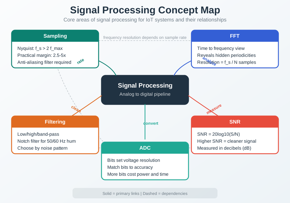
The contract is therefore not "analog bad, digital good." It is a handoff rule. Before the ADC, the design must protect amplitude, bandwidth, source impedance, reference stability, and ground return. At the ADC, it deliberately chooses what amplitude steps and time points will survive. After the ADC, the design must protect codes, timestamps, calibration metadata, and validity flags. A later dashboard can only be as trustworthy as the weakest boundary in that chain.
For example, a vibration sensor on a motor may be accurate at the sensing element but still produce misleading digital data if the analog front end clips peaks, if the anti-alias filter lets high-frequency energy fold into the band of interest, or if the digital packet drops the sampling rate and units. The boundary contract names those failure modes while the design is still reviewable.
That is why good IoT designs digitize as early as possible: the moment a reading becomes bits, it can be copied, transmitted, and stored without further degradation, whereas the raw analog voltage on a long wire keeps picking up interference.
Overview Knowledge Check
Practitioner: Know Which Domain a Signal Is In
Debugging mixed-signal hardware is easier when you always know whether the signal in front of you is analog or digital, because each domain fails differently and responds to different fixes.
| Domain | Represented by | Main enemy | Design lever |
|---|---|---|---|
| Analog | A continuous voltage or current (e.g., 10 mV/°C from a temperature sensor) | Noise pickup, drift, and loading of high-impedance nodes | Shielding, filtering, a buffer amplifier, short traces, clean ground |
| Digital | Codes and logic levels (HIGH/LOW, an ADC's binary output) | Aliasing, timing/setup errors, and occasional bit errors | Adequate sample rate and resolution, correct logic thresholds, retries/checksums |
Worked example — the same wire, two outcomes. A temperature sensor outputs an analog 10 mV/°C signal. Run that raw analog line three metres to the microcontroller and every millivolt of picked-up noise reads as 0.1 °C of false wander. Instead, place a small ADC at the sensor and send the digital code over those three metres: the same electrical interference now has to be larger than the logic noise margin (hundreds of millivolts) before it flips a single bit, so the reading arrives intact.
A "digital" signal is still physically an analog voltage — a 3.3 V logic HIGH is a real 3.3 V. What makes it digital is the shared agreement to interpret a whole band of voltages as 1 and another band as 0. That agreement, plus margin, is the entire source of noise immunity.
A practical boundary review should write down the facts that make the handoff testable: sensor range and source impedance, expected noise and bandwidth, required anti-alias filter corner, ADC reference and resolution, sample rate, logic family, receiver thresholds, cable length, and the units attached to the digital code. If any one of those is implicit, teams debug symptoms instead of the boundary. If they are explicit, the oscilloscope trace, ADC register value, packet field, and cloud record can be compared against the same contract.
Practitioner Knowledge Check
Under the Hood: A Fixed Error Budget vs an Accumulating One
Digitizing does not make a signal perfect — it makes its error bounded and known. The two discretizations each set a hard limit: quantization caps amplitude detail at one LSB (you cannot recover anything finer than Vref / 2^N), and sampling caps time/frequency detail at the Nyquist frequency (you cannot represent anything above fs / 2; higher content folds back as aliasing). Choose the bits and the sample rate at the boundary and you have fixed the error budget for the entire rest of the pipeline.
The amplitude side is a rounding contract. An ideal unipolar ADC with N bits and reference Vref maps a range of input voltages onto 2^N codes, so the unavoidable conversion uncertainty is about half a code step. That error is acceptable only if it is smaller than the measurement tolerance. The time side is a band-limit contract: frequencies above half the sample rate must be removed before the converter, because no downstream digital algorithm can tell whether an aliased component came from the real event or from an under-sampled waveform.
Digital regeneration is a separate but related contract. A receiver does not preserve the exact analog waveform on the wire; it promises to classify voltages below the LOW threshold as 0 and voltages above the HIGH threshold as 1. Noise that stays inside the margin is discarded at the decision point, and the next driver emits a fresh clean LOW or HIGH. Noise that crosses the threshold is no longer "small analog error" — it has become a wrong bit, which is why checksums, retries, and timing margins still matter.
An analog chain has no such boundary. Each amplifier, connector, and long trace adds its own noise, offset, and distortion, and those errors accumulate with every stage — there is no point at which the signal is re-decided and cleaned. This is the deep reason digital dominates modern IoT: it converts an unbounded, growing analog error into a one-time, well-understood conversion error, after which the value is effectively immortal.