27 Applied: PWM vs DAC Output
27.1 Start Simple
Imagine a PWM output that looks correct in firmware but leaves ripple on the analog line. The choice between PWM and DAC is a contract about duty-cycle resolution, frequency, filtering, settling time, and load sensitivity. Start by deciding whether the product needs average power, a stable voltage, or a fast-changing waveform.
27.2 Learning Objectives
After this page, you should be able to:
- Calculate average PWM voltage from duty cycle and supply voltage.
- Compare DAC step size with PWM timer resolution for a selected output range.
- Explain why PWM frequency and resolution trade against each other on counter-based timers.
- Check RC filter cutoff, ripple reduction, and settling time as one design choice.
- Decide when a true DAC is required instead of PWM for an IoT output load.
27.3 Why This Follows DAC and PWM Output
DAC and PWM Output introduces DAC conversion, PWM generation, RC filtering, calculators, and implementation examples. This page turns those ideas into a design contract: what the load actually sees, what timer settings cost, and what error matters most.
Use it when a PWM output flickers, a motor whines, a filtered set-point settles too slowly, a measurement input sees switching ripple, or a team needs to justify using a true DAC rather than another PWM channel.

Phoebe’s Why
The under-the-hood section states two facts about RC-filtered PWM ripple without proving them: it shrinks as \(f_{pwm} \times R \times C\) grows, and it is worst near 50% duty. Both fall out of one simple picture. During the “on” part of each period the capacitor charges toward \(V_{supply}\); during the “off” part it discharges toward 0 V. When the RC time constant is much longer than one PWM period – the normal design regime – each leg of that charge/discharge is nearly a straight line, so the up-swing during \(t_{on}\) and the down-swing during \(t_{off}\) are each proportional to how long that phase lasts. A duty cycle near 50% gives both phases their longest simultaneous share of the period, which is exactly why the ripple peaks there and shrinks toward either extreme.
The Derivation
For \(RC \gg T = 1/f_{pwm}\), the charge step during \(t_{on} = DT\) and the discharge step during \(t_{off} = (1-D)T\) are each linear in time. Setting the steady-state charge step equal to the discharge step gives the peak-to-peak ripple:
\[\Delta V_{pp} \approx (V_{supply} - V_{avg})\frac{DT}{RC} \approx V_{supply}\,\frac{D(1-D)}{f_{pwm}RC}\]
The \(D(1-D)\) term is maximized at \(D = 0.5\) (value \(0.25\)) and falls toward \(0\) at either duty extreme – proving both claims from one formula.
Worked Numbers: This Chapter’s Own 20 kHz, 10 kΩ, 0.22 µF Filter
- Design margin check: \(f_{pwm}RC = 20{,}000 \times 10{,}000 \times 0.22\times10^{-6} = 44\) – comfortably above 1, confirming the linear-ramp approximation this derivation relies on is valid (also consistent with \(RC = 2.2\) ms \(\ll\) the 50 µs PWM period only in the sense that many periods elapse per RC, which is what “\(\gg\)” means here).
- Worst-case ripple (\(D=0.5\)): \(\Delta V_{pp} = 3.3 \times 0.25 / 44 = 0.01875\) V \(\approx 18.8\) mV peak-to-peak on a 3.3 V rail.
- This chapter’s own \(D = 200/255 = 0.784\) example: \(\Delta V_{pp} = 3.3 \times 0.784(0.216) / 44 = 0.0127\) V \(\approx 12.7\) mV – smaller than the 50% case, exactly as the \(D(1-D)\) shape predicts.
- Versus the 12-bit DAC comparison already in this chapter: that DAC’s own LSB is \(0.806\) mV, so even this well-filtered PWM’s ripple is still \(12.7\) to \(18.8\) mV, roughly \(16\) to \(23\times\) larger than one DAC code step – the quantitative reason a true DAC, not just a bigger RC, is what an audio or bias-voltage load actually needs.
Overview: Duty Cycle Is an Average, Not a Voltage
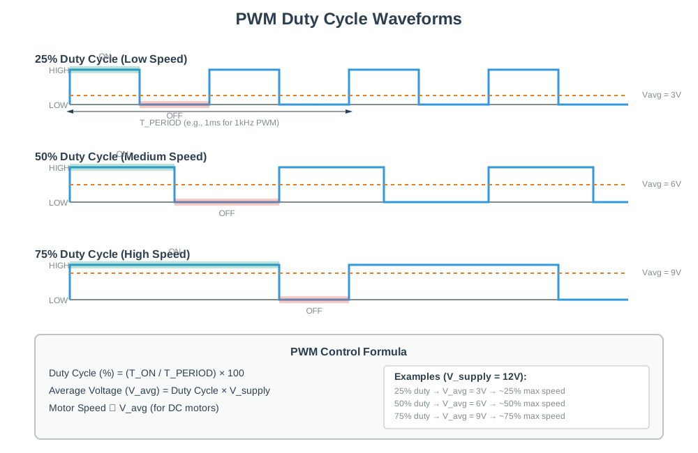
PWM (pulse-width modulation) never outputs an in-between voltage. It switches a pin fully on and fully off, fast, and varies the fraction of time spent on. That fraction is the duty cycle D = t_on / T. Any load that responds slowly compared with the switching period — an LED seen by the eye, a motor's inertia, or an RC filter — reacts only to the average:
Vavg = D × Vsupply.
So a 3.3 V pin at 50% duty averages 1.65 V; at 25% it averages 0.825 V. No true digital-to-analog converter is involved — just a timer toggling a GPIO. The number of distinct duty steps a timer can produce is its resolution: an N-bit PWM has 2^N steps.
Worked example — status LED dimming. Suppose a battery sensor node uses a green LED as a local state indicator and the firmware wants a gentle 30% brightness while the node is sampling. With a 3.3 V GPIO, the timer sets D = 0.30, so the LED path experiences an average drive of about 0.30 × 3.3 = 0.99 V before the LED's own forward-voltage and resistor behavior set the current. The pin is still only ever 0 V or 3.3 V; the apparent in-between level comes from time averaging. If the same node needed to feed a measurement input with a quiet 0.99 V reference, PWM alone would be a poor substitute because the measurement input could see switching ripple. That is where a true DAC or a properly filtered PWM output becomes the right tool.
V_supply in Vavg = D x V_supply.The same arithmetic helps compare DAC resolution. An 8-bit DAC on a 3.3 V reference moves in steps of 3.3 / 255 = 12.9 mV; a 12-bit DAC moves in 3.3 / 4095 = 0.806 mV steps. For a visible LED, 12.9 mV-equivalent duty changes are usually fine. For an analog bias point, an audio waveform, or a calibration stimulus, the smaller 12-bit step can be the difference between a smooth control value and a visible stair-step in the output.
Duty cycle
D = t_on / T, from 0% to 100%. Sets the on-fraction of each period.
Average out
Vavg = D × Vsupply. What a slow load or filter actually sees.
Resolution
An N-bit timer gives 2^N duty steps (256 steps for 8-bit).
Frequency
fpwm must be fast enough that the load cannot follow individual pulses.
Overview Knowledge Check
Practitioner: Frequency and Resolution Trade Against Each Other
On a simple counter-based timer, PWM frequency and resolution are not independent: fpwm = f_clk / 2^N. Asking for more duty steps at a fixed timer clock lowers the PWM frequency, which can drop it into a range where the load does follow the pulses — visible LED flicker, audible motor whine, or servo jitter.
| Load | Typical fpwm | Why |
|---|---|---|
| LED dimming | > ~200 Hz (often ≥ 1 kHz) | Above the eye's flicker-fusion range so no visible flicker |
| DC motor | Often > 20 kHz | Above human hearing to avoid audible whine from the windings |
| Hobby servo | ~50 Hz | The servo expects a fixed ~20 ms frame; the pulse width carries the command |
Worked example — 8-bit PWM at code 200. Duty cycle is D = 200 / 255 = 78.4%. On a 3.3 V rail the averaged output is Vavg = 0.784 × 3.3 = 2.59 V. The finest step this 8-bit PWM can make is one code, 3.3 / 255 ≈ 12.9 mV. Want 16× finer steps? Go to 12-bit PWM (4096 steps) — but at a fixed timer clock that also cuts fpwm by 16×, so check the new frequency still suits the load.
Worked example — timer budget. A microcontroller timer clocked at 10.24 MHz can produce 8-bit PWM at 10.24 MHz / 256 = 40 kHz, safely above the audible band for a small fan driver. Keeping the same timer clock and moving to 12-bit resolution gives 10.24 MHz / 4096 = 2.5 kHz. That is still fine for many LEDs, but it can make motor coils audibly buzz. A practical design would either keep 8-bit resolution for the motor, raise the timer clock if the peripheral allows it, or reserve the finer 12-bit setting for a filtered analog control node that changes slowly.
For a filtered PWM output, include the load in the design. A high-impedance ADC input after an RC filter mainly sees the capacitor voltage, so a 10 kohm and 0.22 uF filter has RC = 2.2 ms and settles to within roughly 1% after about 5RC = 11 ms. That is acceptable for a thermostat set-point updated twice per second. It is too slow for audio, and it may be too sluggish for a control loop that must respond within 2 ms. This is the practitioner check: choose the timer settings, then check the load, filter, ripple, and settling time together.
Practitioner Knowledge Check
Under the Hood: PWM's Spectrum, and When You Need a Real DAC
PWM is not a clean analog source. Its spectrum is the DC average plus strong harmonics at the switching frequency and its multiples. Whatever smooths it — the load's own sluggishness or a deliberate RC low-pass filter — is really just attenuating those harmonics. With an RC filter you pick the cutoff fc = 1 / (2πRC) well below fpwm: the residual ripple shrinks as the product fpwm × R × C grows, and it is largest near 50% duty. The catch is response time: a larger RC means less ripple but slower settling, so smooth-but-sluggish and fast-but-rippled are the two ends of one dial.
A true DAC (an R-2R ladder, or the ESP32's built-in 8-bit DACs on GPIO25/26) instead drives the actual target voltage directly — clean spectrum, no ripple, instant settling — but it costs a dedicated peripheral and usually offers fewer channels and modest resolution. The engineering choice: PWM is free on almost any GPIO and ideal for inertial loads (LEDs, motors, heaters); a real DAC earns its keep when you need a genuinely smooth, fast analog voltage (audio, precise bias, control set-points).
Worked example — ripple versus response. Use 20 kHz PWM, R = 10 kohm, and C = 0.22 uF. The filter cutoff is fc = 1 / (2πRC) = 1 / (2π × 0.0022) ≈ 72 Hz. The first PWM harmonic is therefore about 20,000 / 72 = 278 times above the cutoff, so a first-order RC filter strongly attenuates the switching component. The price is delay: RC = 2.2 ms, and a step change needs about 5RC = 11 ms to settle close to its final value. If firmware updates the set-point every 100 ms, that is comfortable. If it is trying to synthesize a 1 kHz sine wave, it is unusably slow.
Now compare a 12-bit DAC on the same 3.3 V rail. Code 2048 produces about 3.3 × 2048 / 4095 = 1.650 V, and one code changes the output by about 0.806 mV. There is quantization noise and reference noise, but no carrier at 20 kHz that must be filtered out. That is why a DAC is the clean answer for an audio waveform or a bias voltage fed into another analog circuit, while PWM remains the efficient answer when the physical load already averages energy. The under-the-hood test is to ask what error matters more: switching ripple, update latency, step size, output drive, or channel count.